 ChipApex | Global Electronic Components Supplier
SEARCH
Search Product
Search Post
— IC芯片 | 连接器 | 传感器 | 被动器件 —
Search productSearch post
— IC芯片 | 连接器 | 传感器 | 被动器件 —
Consult the customer manager about the wholesale price.
consultation hotline:86-132-6715-2157
email:[email protected]
Contact the product manager for consultation. One-stop consultation is available.
Do you want a lower wholesale price? Please send us your inquiry and we will reply immediately.
The CEL 2SC3585-A is an NPN silicon epitaxial transistor designed for low-noise and small-signal amplifiers in the VHF to UHF bands. It utilizes a direct nitride passivated base surface process (DNP) to achieve excellent noise figures at high current values, providing wide dynamic range and high associated gain. The device operates with a collector-to-emitter voltage of 10 V, a maximum collector current of 35 mA, and total power dissipation of 200 mW. Key electrical characteristics include a typical noise figure of 1.8 dB and a gain bandwidth product of 10 GHz at 2.0 GHz.
Verify that the specific ordering suffix matches the required DC current gain classification. The datasheet defines three distinct hFE ranges: Class R43/Q (50 to 100), Class R44/R (80 to 160), and Class R45/S (125 to 250). Confirm the marking code on the component corresponds to the intended gain bin before finalizing procurement specifications.
Select the appropriate hFE class based on circuit bias requirements. The device requires a collector current between 3 mA and 10 mA for optimal noise and gain performance at 2.0 GHz. Ensure the operating junction temperature remains within the specified -65 °C to +150 °C storage range and that thermal management supports the 200 mW dissipation limit.
This component is manufactured by California Eastern Laboratories (CEL) and is functionally equivalent to the NEC NE68033. Both part numbers share identical electrical specifications and are documented together in the same Renesas Electronics data sheet. The device represents a specialized RF solution for broadband amplification where low noise is critical.
The NEC NE68033 is the primary verified substitute. Both components share identical pinouts, electrical ratings, and package dimensions. Verify that any replacement unit meets the specific hFE classification required for the design.
The device is sorted into three gain bins: Class R43/Q (hFE 50-100), Class R44/R (hFE 80-160), and Class R45/S (hFE 125-250). These are distinguished by specific markings on the package.
The Direct Nitride Passivated Base Surface process allows the transistor to maintain excellent noise figures at higher current values compared to standard processes, resulting in wider dynamic range.
The maximum ratings are 20 V for Collector-to-Base Voltage, 10 V for Collector-to-Emitter Voltage, 1.5 V for Emitter-to-Base Voltage, 35 mA for Collector Current, and 200 mW for Total Power Dissipation.
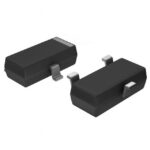 2SC3585-A
The activity of extra discounts on wholesale prices is in full swing…
Please fill in your contact information and we will send you the latest wholesale price list.





