 ChipApex | Global Electronic Components Supplier
SEARCH
Search Product
Search Post
— IC芯片 | 连接器 | 传感器 | 被动器件 —
Search productSearch post
— IC芯片 | 连接器 | 传感器 | 被动器件 —
Consult the customer manager about the wholesale price.
consultation hotline:86-132-6715-2157
email:[email protected]
Contact the product manager for consultation. One-stop consultation is available.
Do you want a lower wholesale price? Please send us your inquiry and we will reply immediately.
The onsemi 2SK3557-6-TB-E is an N-channel JFET in a CP (SC-59/SOT-23) package. It features a drain-to-source voltage of 15 V and a maximum continuous drain current of 50 mA, with power dissipation rated at 200 mW. The device operates within a junction temperature range of -55°C to +150°C. Electrical characteristics include a gate cutoff voltage between -0.3 V and -1.5 V, and a forward transfer admittance of 24 mS to 35 mS. For the Rank 6 variant, the drain current at zero gate-source voltage ranges from 10.0 mA to 20.0 mA.
Verify the specific IDSS rank required for the application, as the 2SK3557 series is classified by drain current ranges. Confirm that the CP package footprint matches the PCB land pattern dimensions provided in the datasheet. Ensure compliance with RoHS directives and verify lead-free soldering requirements during assembly.
Select the 2SK3557-6-TB-E when a lower drain current range (10.0 mA to 20.0 mA) is necessary compared to the higher current Rank 7 variant. Evaluate the 35 mS typical forward transfer admittance against circuit gain requirements. Consider the 10 pF input capacitance for impedance matching in RF stages.
This component belongs to the 2SK3557 family of N-channel JFETs manufactured by onsemi. The family includes multiple ranks differentiated by IDSS values, such as the 2SK3557-7-TB-E which supports a higher current range. All variants share identical electrical limits and physical packaging specifications.
Public documentation lists the 2SK209 as a potential substitute. Verify pinout compatibility and ensure the replacement meets the 15 V breakdown and low-noise requirements. Cross-reference absolute maximum ratings before implementation.
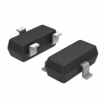 2SK3557-6-TB-E
The activity of extra discounts on wholesale prices is in full swing…
Please fill in your contact information and we will send you the latest wholesale price list.





