 ChipApex | Global Electronic Components Supplier

SEARCH
Search Product
Search Post
— IC芯片 | 连接器 | 传感器 | 被动器件 —
Search productSearch post
— IC芯片 | 连接器 | 传感器 | 被动器件 —
Consult the customer manager about the wholesale price.
consultation hotline:86-132-6715-2157
email:[email protected]
Contact the product manager for consultation. One-stop consultation is available.
Do you want a lower wholesale price? Please send us your inquiry and we will reply immediately.
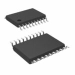
74ACT299MTC is listed in the Shift Registers range at ChipApex. The manufacturer field lists onsemi. Its product description is IC SHIFT/REGISTER STORE 20TSSOP. Review the specifications below when checking this part for your BOM.
The onsemi 74ACT299MTC is an 8-bit universal shift/storage register housed in a 20-lead TSSOP package. It features TTL-compatible inputs and 3-state outputs capable of sourcing or sinking 24 mA. The device operates within a supply voltage range of 4.5 V to 5.5 V and supports temperatures from -40°C to +85°C. Key electrical parameters include a maximum propagation delay of 14 ns at 5.5 V, a quiescent supply current of 40 µA, and input leakage of ±1 µA.
Verify the specific ordering code against the manufacturer's documentation to ensure correct package type and suffix requirements. Confirm that the application environment remains within the specified 4.5 V to 5.5 V supply voltage limits. Ensure thermal management aligns with the -40°C to +85°C operating temperature range. Check for any specific lifecycle status updates regarding availability.
Select this component when an 8-bit universal shift register with common parallel I/O is required. The ACT series provides TTL-compatible inputs, facilitating integration with legacy logic families. The 3-state output capability allows direct connection to system buses without external buffering. Consider the TSSOP package dimensions for PCB layout constraints.
This component belongs to the AC/ACT logic family, designed for high-speed digital applications. The 74ACT299 specifically addresses the need for versatile data handling in compact packages. Its design reduces pin count through multiplexed I/O, making it suitable for space-constrained electronic devices requiring reliable shift and storage functionality.
Direct substitutes include the 74AC299MTC (AC series) and variants from other manufacturers such as STMicroelectronics' 74ACT299M. Verify pin compatibility and electrical specifications before substitution.
Parallel data is loaded by setting mode select inputs S0 and S1 to HIGH while applying data to the I/O pins. The rising edge of the clock pulse transfers this data into the flip-flops.
The MR pin is an active LOW asynchronous reset. When driven LOW, it overrides all other inputs and resets all flip-flop outputs to a LOW state immediately.
Explore related parts through Logic, Integrated Circuits (ICs), all product categories, ChipApex homepage.
 74ACT299MTC

74ACT299MTC is listed in the Shift Registers range at ChipApex. The manufacturer field lists onsemi. Its product description is IC SHIFT/REGISTER STORE 20TSSOP. Review…
Read More
74ACT299MTC is listed in the Shift Registers range at ChipApex. The manufacturer field lists onsemi. Its product description is IC SHIFT/REGISTER STORE 20TSSOP. Review…
Read More
74ACT299MTC is listed in the Shift Registers range at ChipApex. The manufacturer field lists onsemi. Its product description is IC SHIFT/REGISTER STORE 20TSSOP. Review…
Read More
Learn why PTC resistance rises with temperature, how it differs from NTC, and which ratings matter for sensing and protection.
Read More
74ACT299MTC is listed in the Shift Registers range at ChipApex. The manufacturer field lists onsemi. Its product description is IC SHIFT/REGISTER STORE 20TSSOP. Review…
Read More
74ACT299MTC is listed in the Shift Registers range at ChipApex. The manufacturer field lists onsemi. Its product description is IC SHIFT/REGISTER STORE 20TSSOP. Review…
Read More
74ACT299MTC is listed in the Shift Registers range at ChipApex. The manufacturer field lists onsemi. Its product description is IC SHIFT/REGISTER STORE 20TSSOP. Review…
Read More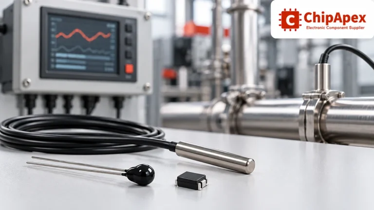
Compare thermistors, RTDs, thermocouples and temperature ICs. Learn how range, accuracy, response, interfaces and mounting affect component selection.
Read More
74ACT299MTC is listed in the Shift Registers range at ChipApex. The manufacturer field lists onsemi. Its product description is IC SHIFT/REGISTER STORE 20TSSOP. Review…
Read More
74ACT299MTC is listed in the Shift Registers range at ChipApex. The manufacturer field lists onsemi. Its product description is IC SHIFT/REGISTER STORE 20TSSOP. Review…
Read More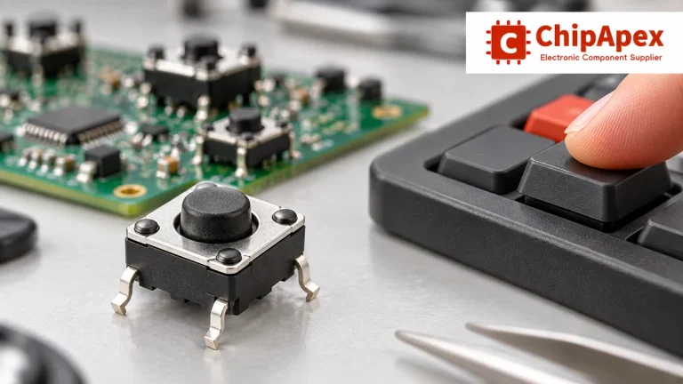
Choose tactile switches by operating force, travel, actuator height, footprint and lifetime. Check debounce, sealing and the assembled button mechanism.
Read More
74ACT299MTC is listed in the Shift Registers range at ChipApex. The manufacturer field lists onsemi. Its product description is IC SHIFT/REGISTER STORE 20TSSOP. Review…
Read More
The activity of extra discounts on wholesale prices is in full swing…
Please fill in your contact information and we will send you the latest wholesale price list.





