 ChipApex | Global Electronic Components Supplier

SEARCH
Search Product
Search Post
— IC芯片 | 连接器 | 传感器 | 被动器件 —
Search productSearch post
— IC芯片 | 连接器 | 传感器 | 被动器件 —
Consult the customer manager about the wholesale price.
consultation hotline:86-132-6715-2157
email:[email protected]
Contact the product manager for consultation. One-stop consultation is available.
Do you want a lower wholesale price? Please send us your inquiry and we will reply immediately.
The AO4619 is a complementary enhancement mode field effect transistor manufactured by Alpha & Omega Semiconductor. It integrates an N-channel and a P-channel MOSFET in a single SOIC-8 package using advanced trench technology. The N-channel device supports a drain-source voltage of 30V with a continuous current of 7.4A at VGS=10V, while the P-channel device handles -30V and -5.2A at VGS=-10V. On-resistance values are less than 24mΩ for the N-channel and 46mΩ for the P-channel at VGS=±10V. Both channels undergo 100% UIS and Rg testing.
Verify component authenticity through authorized distribution channels or direct manufacturer engagement. Confirm RoHS compliance status and specific lot traceability requirements against project specifications. Ensure storage conditions adhere to moisture sensitivity levels defined in the datasheet to prevent package degradation prior to assembly.
Select this component when a matched complementary pair is required for low-voltage power management. The SOIC-8 package offers a compact footprint compared to discrete dual solutions. Evaluate thermal performance based on specific board copper area and ambient airflow, as junction-to-ambient resistance varies significantly with layout design.
This part belongs to the Alpha & Omega Semiconductor complementary MOSFET family. It utilizes trench technology to achieve high performance in a small surface-mount package. The series targets consumer electronics and industrial systems requiring efficient power switching with minimal gate drive requirements.
Direct pin-compatible alternatives within the same manufacturer portfolio include the AO4614B and AO4629. Verify that replacement parts meet identical voltage, current, and thermal ratings before implementation.
The AO4619 is rated for repetitive avalanche energy testing, though specific mJ values depend on pulse width limitations and junction temperature constraints.
The N-channel RDS(ON) is specified at less than 24mΩ at VGS=10V and less than 36mΩ at VGS=4.5V. The P-channel RDS(ON) is less than 46mΩ at VGS=-10V and less than 72mΩ at VGS=-4.5V.
Yes, the N-channel body diode reverse recovery time (trr) is typically 10.5ns, and the P-channel is typically 11ns, measured at IF=7.4A/5.2A with dI/dt=100A/μs.
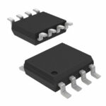 AO4619

The activity of extra discounts on wholesale prices is in full swing…
Please fill in your contact information and we will send you the latest wholesale price list.





