 ChipApex | Global Electronic Components Supplier

SEARCH
Search Product
Search Post
— IC芯片 | 连接器 | 传感器 | 被动器件 —
Search productSearch post
— IC芯片 | 连接器 | 传感器 | 被动器件 —
Consult the customer manager about the wholesale price.
consultation hotline:86-132-6715-2157
email:[email protected]
Contact the product manager for consultation. One-stop consultation is available.
Do you want a lower wholesale price? Please send us your inquiry and we will reply immediately.
The AO4818B is a dual N-channel MOSFET manufactured by Alpha & Omega Semiconductor Inc. utilizing advanced trench technology for low on-resistance and gate charge. It features a drain-source voltage (VDS) of 30V, continuous drain current (ID) of 8A at VGS=10V, and maximum on-resistance (RDS(ON)) of less than 19mΩ at VGS=10V and 26mΩ at VGS=4.5V. The device includes ESD protection and is 100% UIS tested. It operates within a junction temperature range of -55°C to 150°C and is housed in an SOIC-8 surface-mount package.
Verify the specific datasheet revision against the manufacturer's official documentation before implementation. Confirm that the SOIC-8 package dimensions and pinout align with the target PCB footprint. Ensure thermal management strategies account for the specified junction-to-ambient resistance values under actual operating conditions.
Select this component when a dual N-channel configuration is required within a 30V system. The logic-level gate threshold supports efficient driving from standard logic outputs. Evaluate the thermal dissipation requirements based on the specific board copper area and airflow conditions, as the junction-to-ambient resistance varies significantly with layout design.
This part belongs to the AO481 series of dual N-channel MOSFETs produced by Alpha & Omega Semiconductor. The AO4818B specifically targets applications requiring moderate current handling in a compact surface-mount form factor. It complements other devices in the family offering different voltage or current ratings while maintaining consistent packaging standards.
Direct substitutes must match the 30V rating, dual N-channel topology, and SOIC-8 package. Verify that alternative components meet the same RDS(ON) specifications at both 10V and 4.5V gate voltages to ensure equivalent circuit performance.
The absolute maximum gate-source voltage (VGS) is rated at ±20V.
Yes, the device exhibits fast switching times, including a turn-on rise time (tr) of 3.5ns and a turn-off fall time (tf) of 3.5ns, supporting high-frequency PWM applications.
The body diode reverse recovery time (trr) is typically 6ns and maximally 10ns when tested at IF=8A and dI/dt=500A/ms.
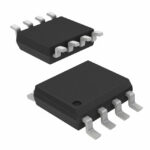 AO4818B

The activity of extra discounts on wholesale prices is in full swing…
Please fill in your contact information and we will send you the latest wholesale price list.





