 ChipApex | Global Electronic Components Supplier

SEARCH
Search Product
Search Post
— IC芯片 | 连接器 | 传感器 | 被动器件 —
Search productSearch post
— IC芯片 | 连接器 | 传感器 | 被动器件 —
Consult the customer manager about the wholesale price.
consultation hotline:86-132-6715-2157
email:[email protected]
Contact the product manager for consultation. One-stop consultation is available.
Do you want a lower wholesale price? Please send us your inquiry and we will reply immediately.
The AO4828L is a dual N-channel enhancement mode field effect transistor manufactured by Alpha & Omega Semiconductor Inc. It utilizes advanced trench MOSFET technology to deliver low on-state resistance and reduced gate charge, making it suitable for load switch and PWM applications. The device features a drain-source voltage of 60V and a continuous drain current of 4.5A at VGS=10V. Key electrical parameters include an on-resistance of less than 56mΩ at VGS=10V and less than 77mΩ at VGS=4.5V. It operates within a junction temperature range of -55°C to 150°C and is housed in an SOIC-8 package.
Verify the specific suffix 'L' against the official datasheet to confirm pinout or thermal specifications match the base AO4828 model. Confirm component availability status as distribution channels may list obsolete inventory. Ensure compliance with RoHS directives if required for the target assembly process.
Select this component when a dual N-channel configuration is required for space-constrained designs. Evaluate the 60V breakdown voltage and 4.5A current rating against circuit demands. Consider the SOIC-8 package dimensions for PCB layout constraints and verify thermal management requirements based on the specified junction-to-ambient resistance values.
The AO4828 belongs to the AOS Dual N-Channel MOSFET family designed for general-purpose power switching. It shares architectural similarities with other trench-based devices in the portfolio but offers specific performance metrics optimized for efficiency. The dual configuration integrates two independent channels within a single compact package to reduce board footprint.
Direct replacements must match the 60V/4.5A dual N-channel specification and SOIC-8 package. Verify equivalent RDS(ON) and gate charge values to maintain switching performance. Cross-reference pinouts carefully as minor variations exist between manufacturers.
The maximum continuous drain current is 4.5A when measured at a gate-source voltage of 10V.
Yes, the device is 100% UIS tested and supports a repetitive avalanche energy of 18 mJ with an inductance of 0.1mH.
The typical total gate charge (Qg) at VGS=10V is 10.5 nC, with a maximum of 10.5 nC listed in the electrical characteristics table.
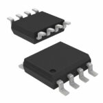 AO4828L

The activity of extra discounts on wholesale prices is in full swing…
Please fill in your contact information and we will send you the latest wholesale price list.





