 ChipApex | Global Electronic Components Supplier

SEARCH
Search Product
Search Post
— IC芯片 | 连接器 | 传感器 | 被动器件 —
Search productSearch post
— IC芯片 | 连接器 | 传感器 | 被动器件 —
Consult the customer manager about the wholesale price.
consultation hotline:86-132-6715-2157
email:[email protected]
Contact the product manager for consultation. One-stop consultation is available.
Do you want a lower wholesale price? Please send us your inquiry and we will reply immediately.
The AO4892 is a dual N-channel MOSFET utilizing trench technology for high-frequency switching. It features a drain-source voltage of 100V and a continuous drain current of 4A at VGS=10V. The on-resistance is less than 68mΩ at VGS=10V and less than 94mΩ at VGS=4.5V. The device operates within a junction temperature range of -55°C to 150°C, with a maximum power dissipation of 2.0W. It includes 100% UIS and Rg testing.
Verify the specific package type and marking code against the manufacturer's latest datasheet revision before ordering. Confirm thermal performance requirements align with the specified junction-to-ambient resistance values under actual board layout conditions. Ensure compliance with RoHS directives if required by the end application.
Select this component for applications requiring efficient high-frequency switching in dual-channel configurations. Consider the 100V rating and 4A continuous current capability when designing boost converters or synchronous rectification circuits. Evaluate thermal management needs based on the 2.0W power dissipation limit and SOIC-8 package constraints.
The AO4892 belongs to Alpha & Omega Semiconductor's lineup of dual N-channel MOSFETs designed for power management applications. It shares the SOIC-8 footprint common to many surface-mount power devices but offers specific electrical characteristics optimized for efficiency in consumer and industrial power supply designs.
Direct replacements include FDC3601N, FDS3601, FDS3912, KDS3601, KDS3912, AO4886, and AON6850. Verify pinout compatibility and electrical parameters such as VDS, ID, and RDS(ON) before substitution.
The maximum gate-source voltage (VGS) is ±20V.
Yes, the device undergoes 100% Unclamped Inductive Switching (UIS) testing.
The typical total gate charge (Qg) at VGS=10V is 6.5nC, with a maximum of 12nC.
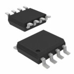 AO4892

The activity of extra discounts on wholesale prices is in full swing…
Please fill in your contact information and we will send you the latest wholesale price list.





