 ChipApex | Global Electronic Components Supplier

SEARCH
Search Product
Search Post
— IC芯片 | 连接器 | 传感器 | 被动器件 —
Search productSearch post
— IC芯片 | 连接器 | 传感器 | 被动器件 —
Consult the customer manager about the wholesale price.
consultation hotline:86-132-6715-2157
email:[email protected]
Contact the product manager for consultation. One-stop consultation is available.
Do you want a lower wholesale price? Please send us your inquiry and we will reply immediately.
The AO6602G is a complementary MOSFET pair from Alpha & Omega Semiconductor, integrating an N-channel and P-channel device in a single TSOP-6 package. The N-channel unit supports a drain-source voltage of 30V with a maximum continuous drain current of 3.5A at VGS=10V, featuring a typical on-resistance below 50mΩ. The P-channel counterpart provides -30V breakdown and -2.7A current capability at VGS=-10V, with a typical on-resistance under 100mΩ. Both transistors utilize Trench Power MOSFET technology to achieve low gate charge and fast switching speeds, making them suitable for high-efficiency power inversion applications.
Verify the component against the official Alpha & Omega Semiconductor datasheet revision 1.0 dated August 2017. Confirm that the received units match the AO6602G part number and TSOP-6 package marking. Ensure compliance with RoHS and Halogen-Free standards as specified by the manufacturer before integration into the final assembly.
Select this component when a matched complementary pair is required for space-constrained designs. The N-channel device offers higher current capacity (3.5A) compared to the P-channel (-2.7A), which may influence circuit symmetry. Verify that the application's thermal environment allows for adequate heat dissipation within the specified junction temperature range of -55°C to 150°C.
This component belongs to the AO6602 series of complementary MOSFETs manufactured by Alpha & Omega Semiconductor. It is designed as a general-purpose solution for replacing discrete N and P-channel pairs in applications requiring synchronized switching characteristics and reduced board footprint.
Direct substitutes include the AO6602L, which is electrically identical but offered as a green product option. Other compatible parts from different manufacturers must be evaluated based on matching voltage ratings, current capabilities, and package dimensions.
The N-channel device supports a maximum continuous drain current of 3.5A when the gate-source voltage is 10V.
Yes, the datasheet includes test circuits and waveforms for Unclamped Inductive Switching (UIS), indicating the device is characterized for this mode of operation.
The typical total gate charge (Qg) for the N-channel device is 4.05 nC when measured at VGS=10V and VDS=15V.
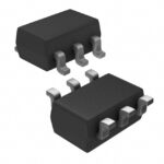 AO6602G

The activity of extra discounts on wholesale prices is in full swing…
Please fill in your contact information and we will send you the latest wholesale price list.





