 ChipApex | Global Electronic Components Supplier

SEARCH
Search Product
Search Post
— IC芯片 | 连接器 | 传感器 | 被动器件 —
Search productSearch post
— IC芯片 | 连接器 | 传感器 | 被动器件 —
Consult the customer manager about the wholesale price.
consultation hotline:86-132-6715-2157
email:[email protected]
Contact the product manager for consultation. One-stop consultation is available.
Do you want a lower wholesale price? Please send us your inquiry and we will reply immediately.
The AO6604 is a complementary enhancement mode MOSFET from Alpha & Omega Semiconductor, integrating an N-channel and P-channel device in a single TSOP-6 package. The N-channel unit provides a drain-source voltage (VDS) of 20V and continuous drain current (ID) of 3.4A at VGS=4.5V, with RDS(ON) below 65mΩ. The P-channel unit offers -20V VDS and -2.5A ID at VGS=-4.5V, with RDS(ON) under 75mΩ. Both transistors feature low gate charge and fast switching characteristics, supporting operation across a junction temperature range of -55°C to 150°C.
Verify the specific ordering suffix against the manufacturer's official documentation to ensure correct packaging and tape-and-reel specifications. Confirm RoHS compliance status and lead time requirements directly with authorized distributors or the manufacturer before placing orders. Ensure the component matches the intended thermal and electrical requirements for the target application.
Select this component when a complementary pair of low-voltage, high-current MOSFETs is required in a minimal footprint. Evaluate the thermal resistance (RθJA) based on the specific PCB copper area and airflow conditions, as the rated power dissipation depends heavily on board design. Ensure gate drive voltages align with the specified thresholds for optimal RDS(ON) performance.
This part belongs to the family of complementary MOSFETs designed by Alpha & Omega Semiconductor. It utilizes advanced trench technology to achieve low on-resistance within a small outline package. The device is engineered specifically for portable electronics and power management systems where size and efficiency are critical constraints.
Potential substitutes include other 20V complementary MOSFETs in TSOP-6 packages, such as the FDMA1032CZ or PJS6601. Verify pinout compatibility, RDS(ON) values, and thermal characteristics before substitution. Cross-reference datasheets to ensure equivalent switching speeds and gate charge parameters match the original design requirements.
The maximum continuous drain current for the N-channel MOSFET is 3.4A when measured at a gate-source voltage of 4.5V.
Yes, the datasheet includes test circuits and waveforms for Unclamped Inductive Switching (UIS), indicating the device is characterized for this condition.
The typical gate threshold voltage (VGS(th)) for the P-channel MOSFET is -0.65V, with a range from -0.4V to -1V.
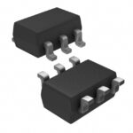 AO6604_001

The activity of extra discounts on wholesale prices is in full swing…
Please fill in your contact information and we will send you the latest wholesale price list.





