 ChipApex | Global Electronic Components Supplier

SEARCH
Search Product
Search Post
— IC芯片 | 连接器 | 传感器 | 被动器件 —
Search productSearch post
— IC芯片 | 连接器 | 传感器 | 被动器件 —
Consult the customer manager about the wholesale price.
consultation hotline:86-132-6715-2157
email:[email protected]
Contact the product manager for consultation. One-stop consultation is available.
Do you want a lower wholesale price? Please send us your inquiry and we will reply immediately.
AO6604L_001 is listed in the FET, MOSFET Arrays range at ChipApex. The manufacturer field lists Alpha & Omega Semiconductor Inc.. Its product description is MOSFET N/P-CH 20V 3.4A 6TSOP. Review the specifications below when checking this part for your BOM.
The AO6604L_001 is a complementary enhancement mode field effect transistor manufactured by Alpha & Omega Semiconductor Inc. It integrates an N-channel and a P-channel MOSFET within a single TSOP-6 package. The N-channel device supports a drain-source voltage of 20V with a continuous drain current of 3.4A at VGS=4.5V, while the P-channel device handles -20V and -2.5A at VGS=-4.5V. Both channels utilize advanced trench technology to achieve low on-resistance values below 65mΩ and 75mΩ respectively at 4.5V gate drive. The component operates within a junction temperature range of -55°C to +150°C.
Verify the specific ordering suffix against the manufacturer's official documentation to confirm exact packaging configuration and marking details. Ensure the selected variant matches the required thermal and electrical specifications for the intended circuit environment before finalizing procurement orders.
Select this component when a matched complementary pair is required for synchronous switching or high-side/low-side control within limited board area. Evaluate the specific gate drive voltage requirements against the provided on-resistance curves to ensure adequate current handling capabilities are met under operating conditions.
This part belongs to the Alpha & Omega Semiconductor complementary MOSFET family designed for low-voltage power management. It serves as a monolithic solution replacing discrete dual-transistor setups, simplifying PCB layout and reducing parasitic inductance in power switching paths.
Direct pin-compatible alternatives include the FDMA1032CZ from ON Semiconductor and the SSF2145CH6 from GOOD-ARK Electronics. Verify that substitute devices meet the same voltage ratings and on-resistance thresholds for equivalent performance.
The maximum junction temperature (TJ) and storage temperature range for the AO6604 is specified as -55°C to +150°C.
The on-resistance increases as the junction temperature rises. Typical characteristics show normalized on-resistance increasing significantly from 25°C to 125°C for both N-channel and P-channel devices.
The typical body diode reverse recovery time (trr) for the N-channel device is 14 ns, with a maximum of 19 ns under test conditions of IF=3.4A and dI/dt=100A/ms.
Explore related parts through FETs, MOSFETs, Transistors, Discrete Semiconductor Products, all product categories.
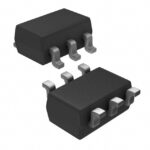 AO6604L_001

The activity of extra discounts on wholesale prices is in full swing…
Please fill in your contact information and we will send you the latest wholesale price list.





