 ChipApex | Global Electronic Components Supplier

SEARCH
Search Product
Search Post
— IC芯片 | 连接器 | 传感器 | 被动器件 —
Search productSearch post
— IC芯片 | 连接器 | 传感器 | 被动器件 —
Consult the customer manager about the wholesale price.
consultation hotline:86-132-6715-2157
email:[email protected]
Contact the product manager for consultation. One-stop consultation is available.
Do you want a lower wholesale price? Please send us your inquiry and we will reply immediately.
The AO6800 is a dual N-channel MOSFET from Alpha & Omega Semiconductor Inc., utilizing advanced trench technology. It features a drain-source voltage (VDS) of 30V and a continuous drain current (ID) of 3.4A at VGS=10V. The on-state resistance (RDS(ON)) is less than 60mΩ at VGS=10V, less than 70mΩ at VGS=4.5V, and less than 90mΩ at VGS=2.5V. Key dynamic parameters include a total gate charge (Qg) of 10nC at VGS=10V and an input capacitance (Ciss) of 235pF. The device operates within a junction temperature range of -55°C to 150°C and is housed in a TSOP6 package.
Verify the specific datasheet revision and manufacturing date code upon ordering. Confirm that the component meets RoHS compliance requirements if necessary for your assembly process. Ensure the supplier provides traceability documentation consistent with Alpha & Omega Semiconductor Inc. standards. Check for any specific handling precautions related to the TSOP6 surface-mount package during soldering.
Select this component when a dual N-channel MOSFET with a 30V rating and approximately 3.4A continuous current capability is required. Consider the low RDS(ON) values at various gate voltages for efficiency optimization. Evaluate the thermal characteristics against your board design, specifically the junction-to-ambient resistance, to ensure adequate heat dissipation without exceeding the maximum junction temperature.
The AO6800 belongs to the AO680 series of dual N-channel MOSFETs manufactured by Alpha & Omega Semiconductor Inc. This series is designed for general-purpose switching applications requiring low on-resistance and fast switching speeds. The AO6800 specifically offers a 30V breakdown voltage, distinguishing it from higher-voltage variants in the broader product line.
Publicly confirmed substitute part numbers are not available in the provided source material. Verify pinout compatibility and electrical specifications before considering alternative manufacturers' components.
The maximum gate-source voltage (VGS) is ±12V.
The typical turn-on delay time (tD(on)) is 3.5 ns.
The body diode reverse recovery charge (Qrr) is typically 2.55 nC when IF=3.4A and dI/dt=100A/ms.
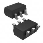 AO6800

The activity of extra discounts on wholesale prices is in full swing…
Please fill in your contact information and we will send you the latest wholesale price list.





