 ChipApex | Global Electronic Components Supplier
SEARCH
Search Product
Search Post
— IC芯片 | 连接器 | 传感器 | 被动器件 —
Search productSearch post
— IC芯片 | 连接器 | 传感器 | 被动器件 —
Consult the customer manager about the wholesale price.
consultation hotline:86-132-6715-2157
email:[email protected]
Contact the product manager for consultation. One-stop consultation is available.
Do you want a lower wholesale price? Please send us your inquiry and we will reply immediately.
The AO8801A is a dual P-channel enhancement mode field effect transistor manufactured by Alpha & Omega Semiconductor Inc. It utilizes advanced trench technology to deliver low on-resistance and gate charge, supporting operation with gate voltages as low as 1.8V. The device features a drain-source voltage of -20V and a continuous drain current of -4.5A at VGS=-10V. On-resistance values are less than 42mΩ at VGS=-4.5V, 54mΩ at VGS=-2.5V, and 68mΩ at VGS=-1.8V. It is housed in an 8-pin TSSOP package and includes ESD protection.
Verify the specific ordering suffix and manufacturer lot codes against the official Alpha & Omega Semiconductor datasheet before procurement. Confirm that the component matches the AO8801A electrical specifications and TSSOP-8 physical dimensions. Ensure compliance with RoHS standards if required by the design specification.
Select this component for applications requiring dual P-channel MOSFETs with logic-level gate drive compatibility. The low on-resistance at VGS=-1.8V makes it suitable for battery-powered devices. Verify thermal dissipation requirements based on the junction-to-ambient resistance of 130°C/W in still air environments.
The AO8801A belongs to the AO8801 family of dual P-channel MOSFETs from Alpha & Omega Semiconductor. It shares similar electrical characteristics with other members of the series but is specifically characterized for its performance at lower gate-source voltages. The device is designed for general-purpose switching applications in portable electronics.
Direct substitutes include the AO8801 and AO8801L, which are electrically identical according to manufacturer documentation. Other dual P-channel MOSFETs with comparable -20V ratings and TSSOP-8 packaging may be considered if pinout and electrical parameters match exactly.
The absolute maximum gate-source voltage (VGS) is ±8V.
Yes, it has low gate charge (Qg max 11nC) and fast switching times (turn-on rise time 9ns), making it suitable for PWM applications.
The maximum on-resistance (RDS(ON)) at VGS=-2.5V and ID=-4A is 54mΩ.
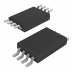 AO8801A
The activity of extra discounts on wholesale prices is in full swing…
Please fill in your contact information and we will send you the latest wholesale price list.





