 ChipApex | Global Electronic Components Supplier
SEARCH
Search Product
Search Post
— IC芯片 | 连接器 | 传感器 | 被动器件 —
Search productSearch post
— IC芯片 | 连接器 | 传感器 | 被动器件 —
Consult the customer manager about the wholesale price.
consultation hotline:86-132-6715-2157
email:[email protected]
Contact the product manager for consultation. One-stop consultation is available.
Do you want a lower wholesale price? Please send us your inquiry and we will reply immediately.
The AOB286L is an N-Channel MOSFET from Alpha & Omega Semiconductor Inc., utilizing Trench technology optimized for high-frequency switching. It features a Drain-Source Voltage (VDS) of 80V and a continuous drain current (ID) of 70A at VGS=10V. The on-resistance (RDS(ON)) is less than 6.0mΩ at VGS=10V and less than 7.9mΩ at VGS=6V. Key dynamic parameters include a total gate charge (Qg) of 44.5nC typ, input capacitance (Ciss) of 3142pF, and turn-on delay time (tD(on)) of 13.5ns. The device supports a maximum junction temperature of 175°C.
Verify the specific package variant required, as the datasheet covers both TO-220 (AOT286L) and surface mount TO-263 (AOB286L). Confirm thermal management requirements align with the specified junction-to-case or junction-to-ambient resistance values based on your PCB design. Ensure compatibility with the 80V rating and 70A current limits for your circuit topology.
Select this component when an 80V N-Channel MOSFET is needed for efficient high-frequency operation. The low gate charge and fast switching times make it suitable for applications prioritizing efficiency. Consider the thermal characteristics carefully; use the junction-to-case data if heatsinking is employed, or junction-to-ambient data for board-level cooling solutions on FR-4 substrates.
This part belongs to the AOT/AOB series of N-Channel MOSFETs manufactured by Alpha & Omega Semiconductor. The 'AOB' suffix specifically denotes the surface-mount TO-263 package variant, while 'AOT' refers to the through-hole TO-220 version. Both share identical electrical specifications but differ in physical mounting and thermal dissipation characteristics.
Direct replacements must match the 80V VDS, 70A ID, and similar RDS(ON) and Qg specifications. Verify that any substitute supports the same TO-263 footprint if space constraints are critical. Check for equivalent avalanche ratings and body diode reverse recovery characteristics to ensure circuit stability.
The maximum junction temperature (TJ) and storage temperature range is -55°C to 175°C.
Yes, the datasheet confirms that the device undergoes 100% UIS testing.
The typical total gate charge (Qg) at VGS=10V is 44.5 nC.
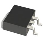 AOB286L
The activity of extra discounts on wholesale prices is in full swing…
Please fill in your contact information and we will send you the latest wholesale price list.





