 ChipApex | Global Electronic Components Supplier

SEARCH
Search Product
Search Post
— IC芯片 | 连接器 | 传感器 | 被动器件 —
Search productSearch post
— IC芯片 | 连接器 | 传感器 | 被动器件 —
Consult the customer manager about the wholesale price.
consultation hotline:86-132-6715-2157
email:[email protected]
Contact the product manager for consultation. One-stop consultation is available.
Do you want a lower wholesale price? Please send us your inquiry and we will reply immediately.
The AOD508 is a 30V N-Channel AlphaMOS power MOSFET from Alpha & Omega Semiconductor Inc. It features a maximum drain-source voltage of 30V and a continuous drain current of 70A at VGS=10V. The device exhibits very low on-resistance, specified as less than 3mW at VGS=10V and less than 4.5mW at VGS=4.5V. It utilizes the latest Trench Power MOSFET technology to achieve high current capability and low gate charge. The component is designed for robust performance in DC/DC converter applications.
Verify the specific package variant required, as the datasheet covers both TO252 (DPAK) and TO-251A (IPAK) configurations. Confirm that the selected part meets the intended thermal dissipation requirements based on the application's board design and ambient temperature conditions. Ensure compliance with RoHS and Halogen-Free standards if mandated by the final product specifications.
Select this component for designs requiring low conduction losses at 30V levels. The low gate charge supports high-frequency operation in switching regulators. Evaluate the thermal management strategy carefully, as the junction-to-ambient resistance varies significantly based on PCB copper area and airflow. The device is suitable for computing and industrial telecom power supplies where efficiency and current density are critical.
This component belongs to the AlphaMOS series from Alpha & Omega Semiconductor Inc., focusing on low-voltage, high-current power switching solutions. The AOD508 specifically targets applications needing robust N-channel MOSFETs with optimized on-resistance. It represents the company's trench technology implementation for cost-effective and high-performance power management in compact form factors.
Check pinout compatibility between TO252 and TO-251A packages if substituting within the same family. Verify that alternative devices meet or exceed the 30V breakdown and 70A current ratings. Ensure the replacement maintains similar gate charge and on-resistance values to preserve circuit efficiency and switching speeds.
The maximum junction and storage temperature range is -55 to 175 °C.
Yes, the datasheet specifies that the device is 100% UIS (Unclamped Inductive Switching) tested.
The gate threshold voltage ranges from a minimum of 1.2V to a maximum of 2.2V at TJ=25°C.
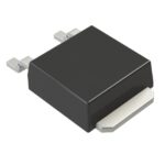 AOD508

The activity of extra discounts on wholesale prices is in full swing…
Please fill in your contact information and we will send you the latest wholesale price list.





