ChipApex | Global Electronic Components Supplier
SEARCH
Search Product
Search Post
— IC芯片 | 连接器 | 传感器 | 被动器件 —
Search productSearch post
— IC芯片 | 连接器 | 传感器 | 被动器件 —
Consult the customer manager about the wholesale price.
consultation hotline:86-132-6715-2157
email:[email protected]
Contact the product manager for consultation. One-stop consultation is available.
Do you want a lower wholesale price? Please send us your inquiry and we will reply immediately.
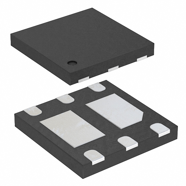
The AON2809 is a dual P-channel MOSFET featuring advanced trench technology for low on-resistance. It operates with a drain-source voltage of -12V and continuous drain current of -2A at VGS=-4.5V. On-resistance is less than 68mΩ at -4.5V, 90mΩ at -2.5V, and 118mΩ at -1.8V. The device includes typical HBM Class 2 ESD protection and is housed in a DFN 2x2A package.
Verify the specific datasheet revision (Rev 0: Nov. 2012) against your design requirements. Confirm that the component meets consumer market standards as it is not authorized for life support devices. Ensure thermal management aligns with the specified junction-to-ambient resistance values.
Select this component for applications requiring compact dual P-channel switching. Evaluate gate drive voltages to ensure RDS(ON) remains within acceptable limits. Consider the DFN 2x2A package size for space-constrained designs. Verify thermal dissipation capabilities under expected load conditions.
This part belongs to Alpha & Omega Semiconductor's lineup of dual MOSFETs designed for efficient power management. It utilizes trench technology to achieve low on-resistance in a small footprint. The device is intended for general consumer electronics applications where space and efficiency are critical factors.
No public confirmed substitute part numbers are available in the provided documentation.
-12V
< 118mΩ
Typical HBM Class 2
 AON2809
The activity of extra discounts on wholesale prices is in full swing…
Please fill in your contact information and we will send you the latest wholesale price list.