ChipApex | Global Electronic Components Supplier
SEARCH
Search Product
Search Post
— IC芯片 | 连接器 | 传感器 | 被动器件 —
Search productSearch post
— IC芯片 | 连接器 | 传感器 | 被动器件 —
Consult the customer manager about the wholesale price.
consultation hotline:86-132-6715-2157
email:[email protected]
Contact the product manager for consultation. One-stop consultation is available.
Do you want a lower wholesale price? Please send us your inquiry and we will reply immediately.
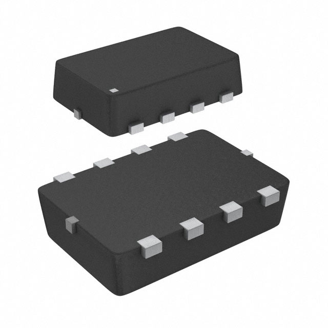
The AON4605 is a complementary enhancement mode MOSFET array manufactured by Alpha & Omega Semiconductor. It integrates an N-channel and a P-channel device within a single DFN 3x2A package. The N-channel component supports a drain-source voltage of 30V with a continuous drain current of 4.3A at VGS=10V, while the P-channel counterpart handles -30V and -3.4A at VGS=-10V. On-resistance values are specified as less than 50mΩ for the N-channel and less than 110mΩ for the P-channel at VGS=10V/-10V. The device utilizes advanced trench technology to achieve low gate charge and high-speed switching capabilities suitable for power inverter applications.
Verify the specific ordering suffix against the manufacturer's official documentation to ensure correct packaging and tape specifications. Confirm that the component meets RoHS compliance standards required for your assembly process. Check for any recent product change notices regarding manufacturing site updates or material substitutions before finalizing procurement plans.
Select this component when a matched pair of N- and P-channel MOSFETs is required for synchronous rectification or half-bridge driving applications. Ensure the operating junction temperature remains within the -55°C to 150°C range. Verify that the gate drive voltage aligns with the specified thresholds for optimal RDS(ON) performance and switching speed.
This part belongs to Alpha & Omega Semiconductor's portfolio of complementary MOSFET arrays. It is designed specifically for the consumer market segment. The manufacturer reserves the right to improve product design, functions, and reliability without notice. It is not authorized for use in life support devices or systems.
Publicly confirmed substitute part numbers are not available in the provided source material. Cross-referencing requires independent verification of pinout compatibility, electrical parameters, and thermal characteristics against the original datasheet.
The maximum junction temperature (TJ) for the AON4605 is 150°C.
The typical total gate charge (Qg) for the N-channel at VGS=10V is 4.05 nC.
The typical body diode reverse recovery time (trr) for the N-channel is 7.5 ns.
 AON4605
The activity of extra discounts on wholesale prices is in full swing…
Please fill in your contact information and we will send you the latest wholesale price list.