ChipApex | Global Electronic Components Supplier
SEARCH
Search Product
Search Post
— IC芯片 | 连接器 | 传感器 | 被动器件 —
Search productSearch post
— IC芯片 | 连接器 | 传感器 | 被动器件 —
Consult the customer manager about the wholesale price.
consultation hotline:86-132-6715-2157
email:[email protected]
Contact the product manager for consultation. One-stop consultation is available.
Do you want a lower wholesale price? Please send us your inquiry and we will reply immediately.
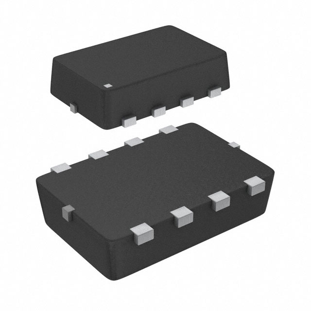
The AON4807 is a dual P-channel enhancement mode field effect transistor manufactured by Alpha & Omega Semiconductor. It utilizes advanced trench MOSFET technology to achieve low on-resistance within a compact DFN 3x2A package. The device features a drain-source voltage of -30V and a continuous drain current of -4A at VGS=-10V. On-resistance is specified as less than 68mΩ at VGS=-10V and less than 105mΩ at VGS=-4.5V. Key dynamic parameters include a total gate charge of 10nC at VGS=-10V and an input capacitance of 290pF. The component operates within a junction temperature range of -55°C to 150°C.
Verify the specific revision status of the datasheet, as the provided documentation indicates Revision 1 from July 2012. Confirm that the component meets RoHS standards and Sony 259 specifications if required by the design. Ensure the ordering suffix matches the exact tape and reel or cut tape requirements for the manufacturing process.
Select this component for applications requiring dual P-channel switching with low on-resistance in a small footprint. Consider the thermal resistance characteristics when designing heat dissipation, as the DFN 3x2A package has limited thermal capacity compared to larger packages. Verify that the gate drive voltage aligns with the specified thresholds for optimal RDS(ON) performance.
The AON4807 belongs to the Alpha & Omega Semiconductor portfolio of power semiconductors. It is part of a series of dual MOSFET arrays designed for consumer electronics and portable devices where space constraints are critical. The manufacturer focuses on providing high-performance trench technology solutions for load management and power control applications.
Check for electrically equivalent dual P-channel MOSFETs with similar voltage and current ratings. Verify pinout compatibility and package dimensions before substitution. Review datasheets for differences in gate charge and thermal resistance to ensure circuit stability.
The maximum continuous drain current is -4A when measured at a gate-source voltage of -10V.
Yes, the device specifies an on-resistance of less than 105mΩ at a gate-source voltage of -4.5V, allowing for logic-level operation.
The component is housed in a DFN 3x2A surface-mount package.
 AON4807
The activity of extra discounts on wholesale prices is in full swing…
Please fill in your contact information and we will send you the latest wholesale price list.