 ChipApex | Global Electronic Components Supplier
SEARCH
Search Product
Search Post
— IC芯片 | 连接器 | 传感器 | 被动器件 —
Search productSearch post
— IC芯片 | 连接器 | 传感器 | 被动器件 —
Consult the customer manager about the wholesale price.
consultation hotline:86-132-6715-2157
email:[email protected]
Contact the product manager for consultation. One-stop consultation is available.
Do you want a lower wholesale price? Please send us your inquiry and we will reply immediately.
The AON5802A is a dual N-channel enhancement mode field effect transistor utilizing advanced trench technology. It features a common-drain configuration suitable for load switching applications. The device operates with gate voltages as low as 2.5V while maintaining a 12V maximum gate-source voltage rating. Key electrical parameters include a drain-source voltage of 30V, continuous drain current of 7.2A at 25°C, and pulsed drain current of 30A. Maximum on-resistance is specified at 16mΩ at VGS=10V and 20mΩ at VGS=4.5V. The component is housed in a DFN 2x5 package with a junction temperature range of -55°C to 150°C.
Verify the specific revision status and manufacturing origin before procurement. Confirm RoHS compliance and lead-free specifications align with project requirements. Check for any recent product change notices that may affect pinout or thermal characteristics. Ensure the supplier provides valid traceability documentation for quality assurance purposes.
Select this component when a dual N-channel MOSFET with low gate drive requirements is needed. The common-drain topology is ideal for high-side switching applications. Consider the thermal resistance values for heat dissipation planning. Verify that the 30V drain-source voltage rating exceeds the maximum circuit voltage under all operating conditions.
The AON5802A belongs to Alpha & Omega Semiconductor's lineup of logic-level power MOSFETs. It is designed for portable and battery-powered applications requiring efficient power management. The DFN 2x5 package offers a compact footprint suitable for space-constrained designs. The device is manufactured using a sub-micron low voltage N-channel process.
Direct substitutes must match the 30V VDS, dual N-channel configuration, and DFN 2x5 package. Verify equivalent RDS(ON) values at similar gate voltages. Ensure thermal performance and pinout compatibility are maintained during replacement.
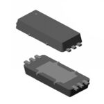 AON5802A
The activity of extra discounts on wholesale prices is in full swing…
Please fill in your contact information and we will send you the latest wholesale price list.





