ChipApex | Global Electronic Components Supplier

SEARCH
Search Product
Search Post
— IC芯片 | 连接器 | 传感器 | 被动器件 —
Search productSearch post
— IC芯片 | 连接器 | 传感器 | 被动器件 —
Consult the customer manager about the wholesale price.
consultation hotline:86-132-6715-2157
email:[email protected]
Contact the product manager for consultation. One-stop consultation is available.
Do you want a lower wholesale price? Please send us your inquiry and we will reply immediately.
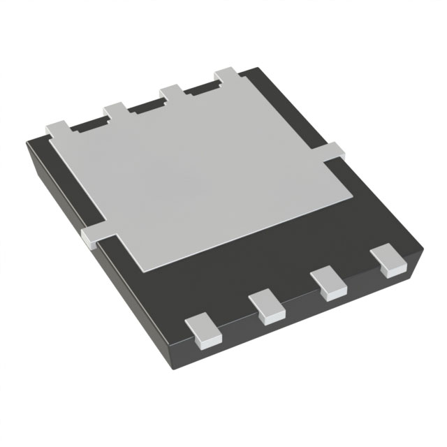
AON6264C is listed in the Single FETs, MOSFETs range at ChipApex. The manufacturer field lists Alpha & Omega Semiconductor Inc.. Its product description is N. Review the specifications below when checking this part for your BOM.
The AON6264C is a 60V N-Channel AlphaSGT™ MOSFET in an 8-DFN (5x6) package. It features a maximum drain-source voltage of 60V and continuous drain current ratings of 24A at 25°C case temperature and 14A at 70°C ambient temperature. The on-resistance is less than 13.2mΩ at VGS=10V and 17.7mΩ at VGS=4.5V. Total gate charge is 21nC at 10V and 10nC at 4.5V. Input capacitance is 895pF, reverse transfer capacitance is 20pF, and output capacitance is 220pF. Thermal resistance junction-to-case is 4.8°C/W, and junction-to-ambient is 55°C/W.
Verify the specific ordering suffix matches the required tape and reel quantity of 3000 units. Confirm that the component meets RoHS 2.0 and halogen-free compliance requirements for your manufacturing process. Ensure the DFN 5x6 package dimensions align with your PCB footprint design rules before finalizing procurement orders.
Select this component when a 60V rating is sufficient and low RDS(ON) is critical for efficiency. The logic level gate drive makes it suitable for 3.3V or 5V control systems. Evaluate thermal performance based on the 55°C/W junction-to-ambient resistance if heatsinking is not utilized in the target application design.
This device belongs to the AlphaSGT™ family from Alpha & Omega Semiconductor Inc., designed for power management applications. It replaces older trench technologies by offering improved figure of merit through reduced gate charge and on-resistance. The part is intended for consumer, telecom, and industrial power supply designs requiring compact surface-mount solutions.
Check datasheets for other AON62xx series parts like AON6262E or AON6266E for pin-compatible alternatives with different current or resistance specifications. Verify that any substitute maintains the same 8-DFN (5x6) package outline and thermal characteristics to ensure board compatibility.
The maximum pulsed drain current (IDM) is 95A.
Yes, the device includes specifications for body diode reverse recovery time (trr) of 17ns and charge (Qrr) of 59nC.
The junction and storage temperature range is -55°C to 150°C.
Explore related parts through FETs, MOSFETs, Transistors, Discrete Semiconductor Products, all product categories.
 AON6264C

The activity of extra discounts on wholesale prices is in full swing…
Please fill in your contact information and we will send you the latest wholesale price list.