ChipApex | Global Electronic Components Supplier
SEARCH
Search Product
Search Post
— IC芯片 | 连接器 | 传感器 | 被动器件 —
Search productSearch post
— IC芯片 | 连接器 | 传感器 | 被动器件 —
Consult the customer manager about the wholesale price.
consultation hotline:86-132-6715-2157
email:[email protected]
Contact the product manager for consultation. One-stop consultation is available.
Do you want a lower wholesale price? Please send us your inquiry and we will reply immediately.
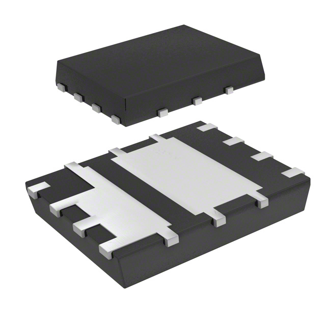
The AON6973A is a dual asymmetric N-channel AlphaMOS MOSFET with a 30V drain-source voltage rating. It integrates an SRFET Schottky diode on the low-side channel (Q2). Q1 supports a continuous drain current of 28A at VGS=10V with RDS(ON) <5.2mΩ, while Q2 supports 32A with RDS(ON) <3.9mΩ. Both channels maintain low resistance at 4.5V drive. The device features 100% UIS and Rg testing, operates from -55°C to 150°C, and uses an 8-DFN (5x6mm) package.
Verify component authenticity by checking manufacturer markings against official datasheet specifications. Confirm RoHS and halogen-free compliance status prior to integration. Ensure thermal design accounts for junction-to-ambient resistance variations based on PCB copper area and airflow conditions specified in the application notes.
Select this component for applications requiring asymmetric current handling where one channel drives higher loads than the other. The integrated body diode reduces external component count in synchronous rectification topologies. Verify that the 30V breakdown voltage aligns with system bus requirements and that the 8-DFN package fits the available footprint constraints.
Manufactured by Alpha & Omega Semiconductor Inc., the AON6973A belongs to the AlphaMOS family utilizing advanced trench technology. It is designed as a complementary pair within a single package to optimize board space and thermal performance for modern compact power electronics designs.
Direct substitutes include AON6970, AON6974, and AON6974A, which share similar 30V dual asymmetric specifications. Verify pinout compatibility and specific RDS(ON) tolerances before swapping to ensure circuit stability.
Q1 and Q2 are asymmetric; Q1 has a lower continuous current rating (28A) and slightly higher on-resistance compared to Q2 (32A), which also features an integrated Schottky diode (SRFET).
Yes, it maintains low on-resistance (<9.5mΩ for Q1 and <6.4mΩ for Q2) when driven at 4.5V, making it suitable for logic-level control applications.
The device undergoes 100% Unclamped Inductive Switching (UIS) testing to verify robustness against avalanche events and diode recovery stress.
 AON6973A
The activity of extra discounts on wholesale prices is in full swing…
Please fill in your contact information and we will send you the latest wholesale price list.