ChipApex | Global Electronic Components Supplier
SEARCH
Search Product
Search Post
— IC芯片 | 连接器 | 传感器 | 被动器件 —
Search productSearch post
— IC芯片 | 连接器 | 传感器 | 被动器件 —
Consult the customer manager about the wholesale price.
consultation hotline:86-132-6715-2157
email:[email protected]
Contact the product manager for consultation. One-stop consultation is available.
Do you want a lower wholesale price? Please send us your inquiry and we will reply immediately.
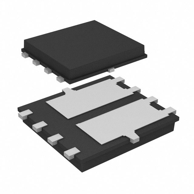
The AOND62930 is a dual N-channel MOSFET utilizing AlphaSGT technology, housed in a DFN5x6 EP2 package. It features a drain-source voltage of 100V and a continuous drain current of 7A at 25°C case temperature. The on-resistance is less than 68mΩ at VGS=10V and less than 94mΩ at VGS=4.5V. Key electrical parameters include a gate threshold voltage ranging from 1.7V to 2.8V, total gate charge of 6.5nC to 12nC at 10V, and input capacitance of 415pF. Thermal characteristics specify a junction-to-case resistance of 17°C/W and a junction-to-ambient resistance of 66°C/W.
Verify the specific ordering suffix and package form against official Alpha & Semiconductor documentation before procurement. Confirm that the component meets all required environmental standards and thermal management specifications for the intended application environment. Ensure compatibility with existing board designs regarding the DFN5x6 EP2 footprint.
Select this component based on its 100V rating and 7A continuous current capability within the DFN5x6 EP2 package. Consider the low on-resistance values at both 10V and 4.5V gate drive voltages for efficiency requirements. Evaluate the thermal resistance parameters to ensure adequate heat dissipation for the target power dissipation levels.
The AOND62930 belongs to the AlphaSGT series of power MOSFETs from Alpha & Omega Semiconductor. It is designed as a dual N-channel device suitable for applications requiring compact packaging and efficient switching. The part utilizes trench technology to achieve low on-resistance and fast switching speeds.
No public confirmed substitute part numbers are available in the provided documentation.
The maximum gate-source voltage is ±20V.
Yes, the datasheet confirms that the device undergoes 100% Unclamped Inductive Switching (UIS) testing.
The body-diode reverse recovery time (trr) is 16ns under specified test conditions.
 AOND62930
The activity of extra discounts on wholesale prices is in full swing…
Please fill in your contact information and we will send you the latest wholesale price list.