ChipApex | Global Electronic Components Supplier

SEARCH
Search Product
Search Post
— IC芯片 | 连接器 | 传感器 | 被动器件 —
Search productSearch post
— IC芯片 | 连接器 | 传感器 | 被动器件 —
Consult the customer manager about the wholesale price.
consultation hotline:86-132-6715-2157
email:[email protected]
Contact the product manager for consultation. One-stop consultation is available.
Do you want a lower wholesale price? Please send us your inquiry and we will reply immediately.
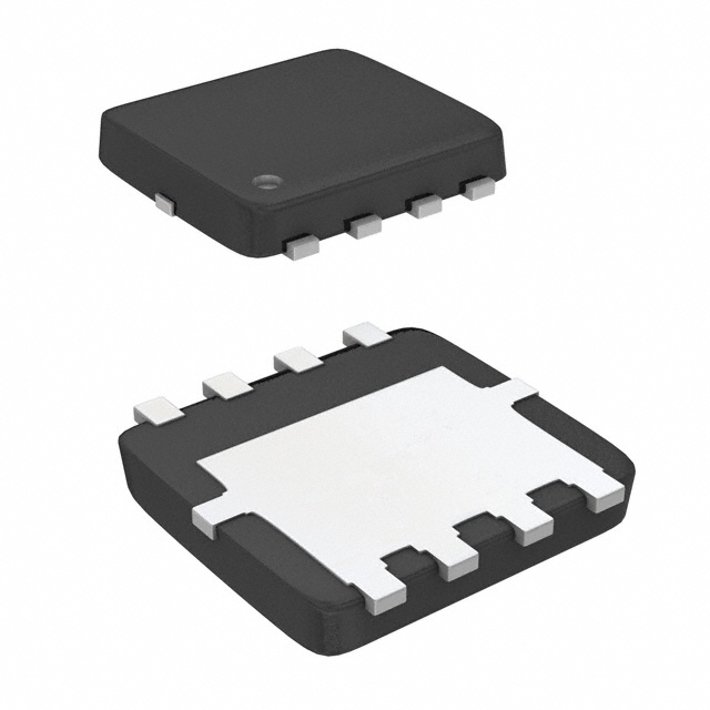
AONR21321 is listed in the Single FETs, MOSFETs range at ChipApex. The manufacturer field lists Alpha & Omega Semiconductor Inc.. Its product description is MOSFET P-CH 30V 24A 8DFN. Review the specifications below when checking this part for your BOM.
The AONR21321 is a P-Channel MOSFET featuring a -30V drain-source voltage and a continuous drain current of -24A at VGS=-10V. It utilizes advanced trench technology to achieve a low on-resistance of less than 16.5mΩ at VGS=-10V and less than 29.5mΩ at VGS=-4.5V. The device is housed in a DFN 3x3_EP package with an exposed pad, offering high current capability and 100% UIS testing for robustness.
Verify the specific ordering suffix matches the required tape and reel quantity of 5000 units. Confirm RoHS and Halogen-Free compliance status if environmental regulations apply to your manufacturing process. Ensure the DFN 3x3_EP package footprint aligns with your PCB design constraints before finalizing procurement.
Select this component when a compact P-Channel solution is required for -30V applications. The low RDS(ON) values support efficient power handling in notebook and battery protection systems. Verify that the gate drive voltage meets the -4.5V or -10V thresholds to utilize the specified on-resistance performance levels effectively.
This part belongs to Alpha & Omega Semiconductor's portfolio of power management components designed for portable electronics. The DFN 3x3_EP package provides a small form factor ideal for space-constrained designs like notebooks. The product emphasizes reliability through comprehensive electrical and thermal testing protocols defined in the datasheet.
No public confirmed substitute part numbers are documented in the source material. Consult official distributor databases for cross-reference data if alternative sourcing is necessary.
Yes, the datasheet confirms that the device undergoes 100% Unclamped Inductive Switching (UIS) testing.
The maximum junction temperature is 150°C, as specified in the absolute maximum ratings and thermal characteristics.
Explore related parts through FETs, MOSFETs, Transistors, Discrete Semiconductor Products, all product categories.
 AONR21321

The activity of extra discounts on wholesale prices is in full swing…
Please fill in your contact information and we will send you the latest wholesale price list.