 ChipApex | Global Electronic Components Supplier

SEARCH
Search Product
Search Post
— IC芯片 | 连接器 | 传感器 | 被动器件 —
Search productSearch post
— IC芯片 | 连接器 | 传感器 | 被动器件 —
Consult the customer manager about the wholesale price.
consultation hotline:86-132-6715-2157
email:[email protected]
Contact the product manager for consultation. One-stop consultation is available.
Do you want a lower wholesale price? Please send us your inquiry and we will reply immediately.
AOSP21311C is listed in the Single FETs, MOSFETs range at ChipApex. The manufacturer field lists Alpha & Omega Semiconductor Inc.. Its product description is MOSFET P-CH 30V 6A 8SOIC. Review the specifications below when checking this part for your BOM.
The AOSP21311C is a surface-mount P-channel MOSFET from Alpha & Omega Semiconductor, housed in an SO-8 package. It features a drain-source voltage (VDS) of -30 V and a continuous drain current (ID) of -6.5 A at VGS=-10V. The device exhibits low on-resistance (RDS(ON)) of less than 42 mΩ at VGS=-10V and less than 64 mΩ at VGS=-4.5V. Thermal performance includes a junction-to-ambient resistance (RqJA) of 85 °C/W and power dissipation capabilities up to 1.6 W at 70°C ambient temperature.
Verify the specific ordering suffix and package configuration against official Alpha & Omega Semiconductor documentation before procurement. Confirm that the component meets RoHS and halogen-free compliance requirements as stated in the datasheet. Ensure that thermal management designs account for the specified junction-to-ambient resistance values under intended operating conditions.
Select this component for applications requiring a -30 V P-channel MOSFET with high current handling. Consider the low RDS(ON) specifications for efficiency in load switching and battery protection circuits. Evaluate the SO-8 package suitability for the target PCB layout and verify that the gate drive voltages align with the specified thresholds for optimal conduction.
This part belongs to the AOSP series of power MOSFETs manufactured by Alpha & Omega Semiconductor. The company specializes in power management ICs and discrete semiconductors. The AOSP21311C is designed for general-purpose switching applications where compact size and efficient power handling are required in consumer electronics and computing systems.
Consult official manufacturer substitution guides or cross-reference databases for verified equivalent parts. Ensure any replacement matches the -30 V rating, SO-8 package dimensions, and electrical characteristics such as RDS(ON) and ID limits.
The maximum drain-source voltage (BVDSS) is -30 V.
Yes, the datasheet confirms that the device undergoes 100% UIS testing.
Explore related parts through FETs, MOSFETs, Transistors, Discrete Semiconductor Products, all product categories.
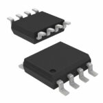 AOSP21311C

The activity of extra discounts on wholesale prices is in full swing…
Please fill in your contact information and we will send you the latest wholesale price list.





