 ChipApex | Global Electronic Components Supplier
SEARCH
Search Product
Search Post
— IC芯片 | 连接器 | 传感器 | 被动器件 —
Search productSearch post
— IC芯片 | 连接器 | 传感器 | 被动器件 —
Consult the customer manager about the wholesale price.
consultation hotline:86-132-6715-2157
email:[email protected]
Contact the product manager for consultation. One-stop consultation is available.
Do you want a lower wholesale price? Please send us your inquiry and we will reply immediately.
The AOTE21115C is a dual P-channel MOSFET array manufactured by Alpha & Omega Semiconductor Inc. It utilizes Trench Power MOSFET technology to achieve low on-resistance and gate charge characteristics. The device features a drain-source voltage of -20V and supports continuous drain currents up to -4.9A at VGS=-4.5V. On-resistance values are specified as less than 44mΩ at VGS=-4.5V, 57mΩ at VGS=-2.5V, and 77mΩ at VGS=-1.8V. It is housed in an 8-TSSOP surface-mount package with a maximum junction temperature rating of 150°C.
Verify the specific ordering suffix against official manufacturer documentation to ensure correct packaging format. Confirm that the component meets RoHS and Halogen-Free compliance requirements for your assembly process. Cross-reference the datasheet revision date to validate electrical parameters before finalizing procurement specifications.
Evaluate thermal resistance values based on the specific PCB copper area and airflow conditions. Ensure gate drive voltages align with the specified thresholds for optimal RDS(ON) performance. Consider the maximum pulsed drain current limits when designing for transient load conditions.
This component belongs to the AOTE series of dual P-channel MOSFET arrays from Alpha & Omega Semiconductor. It is designed for applications requiring two independent channels in a small footprint. The device complements other power management solutions by providing integrated switching capabilities.
Check for compatible dual P-channel MOSFETs with similar -20V ratings and comparable RDS(ON) specifications. Verify pinout compatibility with the 8-TSSOP package before substitution.
The device provides typical ESD protection rated at HBM Class 2.
RDS(ON) increases as the magnitude of VGS decreases, measured at <44mΩ at -4.5V, <57mΩ at -2.5V, and <77mΩ at -1.8V.
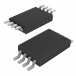 AOTE21115C
The activity of extra discounts on wholesale prices is in full swing…
Please fill in your contact information and we will send you the latest wholesale price list.





