 ChipApex | Global Electronic Components Supplier
SEARCH
Search Product
Search Post
— IC芯片 | 连接器 | 传感器 | 被动器件 —
Search productSearch post
— IC芯片 | 连接器 | 传感器 | 被动器件 —
Consult the customer manager about the wholesale price.
consultation hotline:86-132-6715-2157
email:[email protected]
Contact the product manager for consultation. One-stop consultation is available.
Do you want a lower wholesale price? Please send us your inquiry and we will reply immediately.
The AT17F080A-30QC is an 8-Mbit serial configuration flash memory designed for Field Programmable Gate Arrays (FPGAs). It operates at a supply voltage of 3.3V with 5.0V tolerant I/O pins and supports maximum clock frequencies up to 33MHz during download. The device features In-System Programming via a 2-wire bus, low-power standby mode, and endurance of 100,000 write cycles. It is available in 20-lead PLCC packages.
Verify the package type matches the required design footprint, as this part number specifically denotes the 20-lead PLCC option. Confirm that the industrial temperature range (-40°C to +85°C) meets system requirements. Ensure programming tools support the 2-wire ISP interface for field updates. Check for end-of-life status or obsolescence notices from the manufacturer before finalizing procurement plans.
Select this component when configuring Altera SRAM-based FPGAs requiring non-volatile storage. It offers direct interface compatibility with FPGA control signals without external controllers. Consider the 20-lead PLCC package for through-hole mounting needs. Verify that the 3.3V operation aligns with the target FPGA's power domain and that the 5.0V tolerant inputs are necessary for interfacing.
This device belongs to the AT17FxxxA series of In-System Programmable Configuration PROMs. It serves as a cost-effective solution for storing configuration programs for FPGAs. The series includes variants like the AT17F040A for 4-Mbit capacity. These configurators utilize a simple serial-access procedure to configure one or more FPGA devices automatically upon power-up.
AT17F080A-30JU
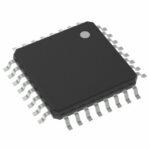 AT17F080A-30QC
The activity of extra discounts on wholesale prices is in full swing…
Please fill in your contact information and we will send you the latest wholesale price list.





