 ChipApex | Global Electronic Components Supplier
SEARCH
Search Product
Search Post
— IC芯片 | 连接器 | 传感器 | 被动器件 —
Search productSearch post
— IC芯片 | 连接器 | 传感器 | 被动器件 —
Consult the customer manager about the wholesale price.
consultation hotline:86-132-6715-2157
email:[email protected]
Contact the product manager for consultation. One-stop consultation is available.
Do you want a lower wholesale price? Please send us your inquiry and we will reply immediately.
The BB184,115 is a silicon varactor diode manufactured by NXP Semiconductors. It is designed for RF tuning applications in VHF and UHF frequency bands. The device features a single PN junction with a capacitance range typically spanning from approximately 2 pF to 30 pF, depending on the applied reverse bias voltage. Key electrical parameters include a maximum reverse voltage rating of 30 V and a low series resistance to minimize insertion loss. The component is housed in a compact surface-mount package, specifically the SOD57 (SC-90) outline, facilitating automated assembly and integration into space-constrained circuit boards.
Verify the specific suffix '115' against the official NXP datasheet to confirm the exact packaging type and tape/reel specifications. Ensure the component meets RoHS compliance requirements if mandated by the target application standards. Cross-reference the ordering code with current availability status as legacy components may have limited supply chains.
Select this component based on the required capacitance ratio and Q-factor at the operating frequency. Evaluate the parasitic series resistance impact on circuit efficiency. Confirm that the package dimensions align with the PCB footprint design rules and that the thermal characteristics are suitable for the expected power dissipation levels in the final assembly.
This component belongs to the family of silicon varactor diodes used for electronic tuning. It serves as a critical passive element in analog RF front-ends, replacing mechanical capacitors for dynamic frequency adjustment. Its performance is defined by the non-linear capacitance-voltage characteristic, enabling precise control over resonant frequencies in communication systems.
Consult the official replacement guide for equivalent varactor diodes with similar C-V curves and voltage ratings. Verify pin compatibility and package dimensions before substituting with alternative manufacturers' parts to ensure seamless integration without redesigning the PCB layout.
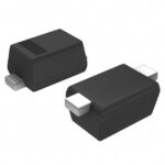 BB184,115
The activity of extra discounts on wholesale prices is in full swing…
Please fill in your contact information and we will send you the latest wholesale price list.





