 ChipApex | Global Electronic Components Supplier

SEARCH
Search Product
Search Post
— IC芯片 | 连接器 | 传感器 | 被动器件 —
Search productSearch post
— IC芯片 | 连接器 | 传感器 | 被动器件 —
Consult the customer manager about the wholesale price.
consultation hotline:86-132-6715-2157
email:[email protected]
Contact the product manager for consultation. One-stop consultation is available.
Do you want a lower wholesale price? Please send us your inquiry and we will reply immediately.
The BC817K-25HR is an NPN general-purpose transistor from the Nexperia BC817KH series, housed in a small SOT23 (TO-236AB) Surface-Mounted Device plastic package. It features a collector-emitter voltage of 45 V and a continuous collector current of 500 mA. The device supports high-temperature applications up to 175 °C and offers three current gain selections; the -25H variant provides a DC current gain range of 160 to 400 at VCE = 1 V and IC = 100 mA. Key electrical characteristics include a collector-base breakdown voltage of 50 V, a peak collector current of 1 A for single pulses, and a transition frequency of 100 MHz.
Verify the specific ordering suffix against the official Nexperia BC817KH series datasheet to confirm package type and binning. Ensure the procurement channel sources directly from authorized distributors or Nexperia to guarantee component authenticity and traceability. Cross-reference the marking code with the manufacturer's documentation to validate the part number before integration into production lines.
Select the BC817K-25HR when a moderate DC current gain between 160 and 400 is required for general-purpose NPN switching tasks. Consider this component for designs requiring operation at elevated temperatures up to 175 °C. Evaluate the SOT23 package constraints regarding thermal resistance and PCB footprint dimensions during the layout phase to ensure adequate heat dissipation under maximum load conditions.
This component belongs to the BC817KH series of NPN general-purpose transistors manufactured by Nexperia. The series includes variants with different current gain bins (-16H, -25H, -40H) to accommodate various amplification requirements. All members share the same SOT23 physical package and core electrical ratings, differing primarily in their hFE classification ranges.
Direct functional substitutes within the same family include BC817K-16H and BC817K-40H, which share identical packages and voltage/current ratings but offer different DC current gain ranges. Verify that the alternative gain bin meets the specific amplification requirements of the target circuit design.
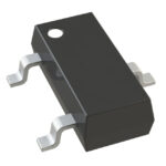 BC817K-25HR

The activity of extra discounts on wholesale prices is in full swing…
Please fill in your contact information and we will send you the latest wholesale price list.





