 ChipApex | Global Electronic Components Supplier
SEARCH
Search Product
Search Post
— IC芯片 | 连接器 | 传感器 | 被动器件 —
Search productSearch post
— IC芯片 | 连接器 | 传感器 | 被动器件 —
Consult the customer manager about the wholesale price.
consultation hotline:86-132-6715-2157
email:[email protected]
Contact the product manager for consultation. One-stop consultation is available.
Do you want a lower wholesale price? Please send us your inquiry and we will reply immediately.
The BF1009SE6327HTSA1 is a silicon N-channel MOSFET tetrode designed for low noise and high gain applications in controlled input stages up to 1 GHz. It features an integrated biasing network and operates at a voltage of 9 V. The device provides a typical power gain of 22 dB and a noise figure of 1.4 dB at 800 MHz. Key electrical parameters include a drain-source breakdown voltage of 12 V, continuous drain current of 25 mA, and forward transconductance of 30 mS. It is qualified according to AEC Q101 standards.
Verify the specific package variant (SOT143 or SOT143R) required for the assembly process. Confirm RoHS compliance status as standard packages are lead-free. Ensure handling precautions for ESD-sensitive devices are followed during storage and installation. Check availability of Pb-containing options only through special request if necessary.
Select this component when designing RF stages requiring high gain and low noise within a 9 V operating range. Consider the integrated biasing network to reduce external component count. Evaluate thermal resistance limits based on the expected ambient temperature and power dissipation requirements. Ensure the application frequency does not exceed the 1 GHz operational limit.
This part belongs to Infineon's silicon N-channel MOSFET tetrode family. These devices are engineered specifically for radio frequency applications where high gain and low noise are critical. The integration of the biasing network distinguishes it from standard MOSFETs, offering a compact solution for RF front-end designs.
No official substitutes are listed in the documentation. When evaluating alternatives, match the N-channel tetrode configuration, 12 V breakdown voltage, and SOT143/SOT143R package dimensions. Verify that replacement components meet the same AEC Q101 qualification and RF performance specifications.
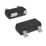 BF1009SE6327HTSA1
The activity of extra discounts on wholesale prices is in full swing…
Please fill in your contact information and we will send you the latest wholesale price list.





