ChipApex | Global Electronic Components Supplier
SEARCH
Search Product
Search Post
— IC芯片 | 连接器 | 传感器 | 被动器件 —
Search productSearch post
— IC芯片 | 连接器 | 传感器 | 被动器件 —
Consult the customer manager about the wholesale price.
consultation hotline:86-132-6715-2157
email:[email protected]
Contact the product manager for consultation. One-stop consultation is available.
Do you want a lower wholesale price? Please send us your inquiry and we will reply immediately.
The BF1201,215 is an N-channel dual-gate PoLo MOS-FET manufactured by NXP Semiconductors. It features a short channel design with high forward transfer admittance to input capacitance ratio. The device operates with a drain-source voltage of 10 V and a continuous drain current of 30 mA. Total power dissipation is rated at 200 mW. Forward transfer admittance ranges from 23 to 35 mS. Input capacitance at gate 1 is typically 2.6 pF. Reverse transfer capacitance is 15 to 30 fF at 1 MHz. Noise figure is 11.8 dB at 400 MHz. Operating junction temperature reaches 150 °C.
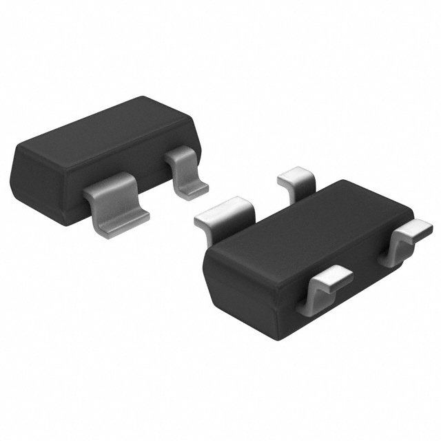
Verify the specific suffix for the BF1201 series to ensure correct package selection. The BF1201 uses SOT143B, BF1201R uses SOT143R, and BF1201WR uses SOT343R. Confirm pinout orientation as reverse pinning variants exist. Check latest product status on manufacturer website as specifications may change. Ensure anti-static handling protocols are followed during transport and assembly.
Select based on required operating frequency and noise figure requirements. Consider thermal resistance values which vary by package type. Verify gain reduction characteristics match AGC control needs. Evaluate cross-modulation input levels for signal integrity in professional communications. Ensure supply voltage constraints align with the 3 to 9 V operational range specified for target applications.
This component belongs to the N-channel dual-gate PoLo MOS-FET family including BF1201, BF1201R, and BF1201WR. These devices share similar electrical characteristics but differ in physical packaging. The family is designed for low noise amplification in radio frequency circuits. They utilize silicon technology for stable operation across varying temperatures.
BF1201R (SOT143R package) and BF1201WR (SOT343R package) offer equivalent electrical performance with different form factors. Pin configurations differ significantly between standard and reverse pinning versions. Direct substitution requires verifying package dimensions and pin numbering compatibility with existing PCB layouts.
Integrated diodes between gates and source protect the device against excessive input voltage surges.
The partly internal self-biasing circuit ensures good cross-modulation performance during automatic gain control and provides good DC stabilization.
The maximum operating junction temperature is 150 °C.
 BF1201,215
The activity of extra discounts on wholesale prices is in full swing…
Please fill in your contact information and we will send you the latest wholesale price list.