 ChipApex | Global Electronic Components Supplier
SEARCH
Search Product
Search Post
— IC芯片 | 连接器 | 传感器 | 被动器件 —
Search productSearch post
— IC芯片 | 连接器 | 传感器 | 被动器件 —
Consult the customer manager about the wholesale price.
consultation hotline:86-132-6715-2157
email:[email protected]
Contact the product manager for consultation. One-stop consultation is available.
Do you want a lower wholesale price? Please send us your inquiry and we will reply immediately.
The BF1201WR,135 is an N-channel dual-gate PoLo MOS-FET manufactured by NXP Semiconductors. It features a short channel design with high forward transfer admittance to input capacitance ratio. The device operates with a drain-source voltage of 10 V and a continuous drain current of 30 mA. Total power dissipation is rated at 200 mW. Key electrical parameters include a typical noise figure of 11.8 dB at 400 MHz and a forward transfer admittance ranging from 23 to 35 mS. The component is housed in the SOT343R plastic surface-mounted package.
Verify the specific ordering suffix
Select this component for designs requiring low-noise amplification in VHF/UHF bands. Ensure the circuit supports the specified 10 V drain-source voltage limit. Verify thermal management capabilities for the SOT343R package to maintain junction temperature within the 150 °C operating range. Confirm that the dual-gate architecture aligns with the required AGC and impedance matching strategies.
This part belongs to the BF1201 series of N-channel dual-gate PoLo MOS-FETs. Variants include BF1201 (SOT143B) and BF1201R (SOT143R). The BF1201WR specifically utilizes the SOT343R package. These devices are designed for RF signal processing where low noise and stable gain control are critical.
Direct substitutes are not explicitly listed in the provided documentation. Engineers should evaluate other N-channel dual-gate MOS-FETs from NXP or compatible manufacturers that match the SOT343R footprint and electrical specifications.
Gate 2 serves as the control terminal for the amplifier's gain, enabling Automatic Gain Control (AGC) functionality while Gate 1 acts as the primary signal input.
Integrated diodes located between the gates and the source provide protection against excessive input voltage surges.
The maximum operating junction temperature (Tj) is 150 °C.
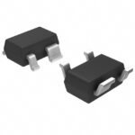 BF1201WR,135
The activity of extra discounts on wholesale prices is in full swing…
Please fill in your contact information and we will send you the latest wholesale price list.





