 ChipApex | Global Electronic Components Supplier
SEARCH
Search Product
Search Post
— IC芯片 | 连接器 | 传感器 | 被动器件 —
Search productSearch post
— IC芯片 | 连接器 | 传感器 | 被动器件 —
Consult the customer manager about the wholesale price.
consultation hotline:86-132-6715-2157
email:[email protected]
Contact the product manager for consultation. One-stop consultation is available.
Do you want a lower wholesale price? Please send us your inquiry and we will reply immediately.
The BF1203,115 is a dual N-channel dual-gate MOS-FET in a SOT363 package. It integrates two low-noise amplifiers with shared source and Gate 2 leads. Key electrical parameters include a drain-source voltage of 10 V and a DC drain current of 30 mA per amplifier. Forward transfer admittance ranges from 23 mS to 40 mS depending on the specific amplifier section. Input capacitance at Gate 1 varies between 1.7 pF and 3.1 pF. Noise figures are specified as low as 0.9 dB at 400 MHz for Amplifier b.
Verify the component status via official NXP channels before design finalization. Confirm the specific ordering suffix matches the required tape and reel configuration. Ensure electrostatic discharge precautions are observed during handling. Cross-reference the latest datasheet revision to confirm pinout consistency with existing designs.
Select this component for high-frequency signal paths requiring independent gain control via the second gate. The device offers high forward transfer admittance suitable for VHF/UHF bands. Consider the thermal resistance characteristics when designing heat dissipation strategies for dense PCB layouts.
This discrete semiconductor belongs to NXP's portfolio of RF small-signal MOSFETs. It utilizes silicon technology and is designed for surface-mount assembly. The device represents a specialized solution for analog front-end processing in broadcast and communication hardware.
Consult official substitution lists for verified equivalents. Generic replacements may not match the specific dual-gate architecture or cross-modulation performance metrics required for AGC stability.
The two amplifiers share common source and Gate 2 leads, while maintaining separate Gate 1 inputs and Drain outputs.
Integrated diodes between the gates and source protect the device against excessive input voltage surges.
The transistor is encapsulated in a SOT363 micro-miniature plastic surface-mounted package.
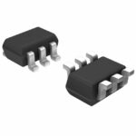 BF1203,115
The activity of extra discounts on wholesale prices is in full swing…
Please fill in your contact information and we will send you the latest wholesale price list.





