 ChipApex | Global Electronic Components Supplier
SEARCH
Search Product
Search Post
— IC芯片 | 连接器 | 传感器 | 被动器件 —
Search productSearch post
— IC芯片 | 连接器 | 传感器 | 被动器件 —
Consult the customer manager about the wholesale price.
consultation hotline:86-132-6715-2157
email:[email protected]
Contact the product manager for consultation. One-stop consultation is available.
Do you want a lower wholesale price? Please send us your inquiry and we will reply immediately.
The BF1205 is a dual N-channel dual gate MOS-FET in an SOT363 package. It integrates two low noise gain controlled amplifiers with shared source and gate leads. One amplifier features fully integrated bias, while the other has partly integrated bias. The device includes an internal switch operated by the gate 1 bias of amplifier b to reduce external components. Key electrical parameters include a drain-source voltage limit of 10 V, a DC drain current of 30 mA, and total power dissipation of 200 mW. Forward transfer admittance is typically 63 mS at 12 mA drain current. Input capacitance ranges from 1.8 pF to 2.5 pF depending on the amplifier section.
Verify the specific ordering suffix to confirm packaging format, as standard designations may vary between tape-and-reel and cut-tape options. Confirm the component status, as availability can change over time. Ensure the sourcing channel provides valid manufacturer documentation to verify authenticity. Check for any specific handling requirements related to electrostatic discharge protection during transport and assembly processes.
Select this component for designs requiring dual independent low noise amplification in a compact surface-mount footprint. The integrated switching capability simplifies circuit topology by reducing external control logic requirements. Consider the thermal resistance characteristics when designing heat dissipation strategies for high ambient temperatures. Verify that the operating frequency range aligns with the specified forward transfer admittance and noise figure performance curves.
This device belongs to the discrete semiconductor category, specifically RF MOSFET transistors manufactured by NXP Semiconductors. It is designed for radio frequency applications where low noise and high linearity are critical. The SOT363 package allows for efficient use of printed circuit board space in portable and professional electronic devices.
Check for direct pin-compatible alternatives within the same manufacturer's portfolio that offer similar dual-gate configurations. Verify that any substitute component matches the SOT363 package dimensions and electrical specifications for drain-source voltage and current ratings.
The internal switch is operated by the gate 1 bias of amplifier b. When VGG is set to 5 V, amplifier a is turned off and amplifier b is on. When VGG is 0 V, amplifier a is on and amplifier b is off.
The transistor includes integrated diodes between the gates and the source to protect against excessive input voltage surges.
The typical forward transfer admittance is 63 mS when the drain current is 12 mA and the junction temperature is 25 °C.
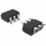 BF1205,135
The activity of extra discounts on wholesale prices is in full swing…
Please fill in your contact information and we will send you the latest wholesale price list.





