ChipApex | Global Electronic Components Supplier
SEARCH
Search Product
Search Post
— IC芯片 | 连接器 | 传感器 | 被动器件 —
Search productSearch post
— IC芯片 | 连接器 | 传感器 | 被动器件 —
Consult the customer manager about the wholesale price.
consultation hotline:86-132-6715-2157
email:[email protected]
Contact the product manager for consultation. One-stop consultation is available.
Do you want a lower wholesale price? Please send us your inquiry and we will reply immediately.
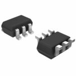
The BF1210,115 is a dual N-channel dual-gate MOSFET amplifier in a SOT363 package. It integrates two low-noise gain-controlled amplifiers with shared source and gate2 leads. The device features internal bias circuits for DC stabilization and integrated protection diodes between gates and source. Key electrical parameters include a drain-source voltage of 6 V, drain current of 30 mA, and total power dissipation of 180 mW. Forward transfer admittance ranges from 26 to 43 mS depending on the amplifier channel and bias conditions.
Verify component authenticity through authorized NXP Semiconductors distributors or certified partners. Confirm the specific ordering suffix matches the required packaging configuration. Ensure handling procedures adhere to ElectroStatic Discharge (ESD) sensitivity guidelines during transport and assembly to prevent device damage.
Select this component for designs requiring compact integration of dual RF amplifiers with shared control lines. Evaluate thermal resistance characteristics against system heat dissipation requirements. Verify that the 6 V maximum drain-source voltage aligns with the target supply voltage constraints for VHF and UHF tuner stages.
This device belongs to the NXP dual-gate MOSFET family designed for radio frequency signal processing. It serves as a specialized active component for tuning and amplification stages in broadcast and communication hardware. The SOT363 package allows for surface-mount integration in space-constrained electronic assemblies.
BF1210WR,115
 BF1210,115
The activity of extra discounts on wholesale prices is in full swing…
Please fill in your contact information and we will send you the latest wholesale price list.