 ChipApex | Global Electronic Components Supplier
SEARCH
Search Product
Search Post
— IC芯片 | 连接器 | 传感器 | 被动器件 —
Search productSearch post
— IC芯片 | 连接器 | 传感器 | 被动器件 —
Consult the customer manager about the wholesale price.
consultation hotline:86-132-6715-2157
email:[email protected]
Contact the product manager for consultation. One-stop consultation is available.
Do you want a lower wholesale price? Please send us your inquiry and we will reply immediately.
The BF2040E6814HTSA1 is a silicon N-channel MOSFET tetrode in the SOT-143 package. It operates at a drain-source voltage of 8 V with a continuous drain current of 40 mA and total power dissipation of 200 mW. The device provides a typical power gain of 23 dB and a noise figure of 1.6 dB at 800 MHz, operating under a 5 V supply. Key electrical parameters include a breakdown voltage of 10 V, forward transconductance of 42 mS, and gate-source pinch-off voltages between 0.3 V and 0.7 V.
Verify component authenticity through authorized Infineon channels or certified distributors. Confirm the specific E6814 suffix matches the required SOT-143 packaging variant. Ensure handling precautions are observed due to electrostatic discharge sensitivity. Validate RoHS compliance status against current regulatory requirements before integration into production assemblies.
Select this component when designing RF stages requiring high gain and low noise figures around 800 MHz. The dual-gate architecture supports precise gain control applications. Consider the 8 V maximum drain-source voltage and 200 mW power dissipation limits during thermal management planning. Verify that the SOT-143 footprint aligns with the target PCB layout constraints.
This part belongs to the BF2040 series, which includes variants in SOT143R and SOT343 packages. All series members share identical electrical characteristics but differ in physical pin configurations and mechanical dimensions. The E6814 suffix specifically identifies the standard SOT143 surface-mount package configuration.
Direct replacements must match the SOT-143 package and maintain equivalent RF performance metrics. Verify that alternative components support the same 8 V drain-source voltage and 40 mA current ratings. Cross-reference pinout assignments carefully, as other package variants within the series utilize different terminal mappings.
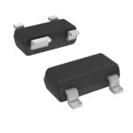 BF2040E6814HTSA1
The activity of extra discounts on wholesale prices is in full swing…
Please fill in your contact information and we will send you the latest wholesale price list.





