ChipApex | Global Electronic Components Supplier
SEARCH
Search Product
Search Post
— IC芯片 | 连接器 | 传感器 | 被动器件 —
Search productSearch post
— IC芯片 | 连接器 | 传感器 | 被动器件 —
Consult the customer manager about the wholesale price.
consultation hotline:86-132-6715-2157
email:[email protected]
Contact the product manager for consultation. One-stop consultation is available.
Do you want a lower wholesale price? Please send us your inquiry and we will reply immediately.
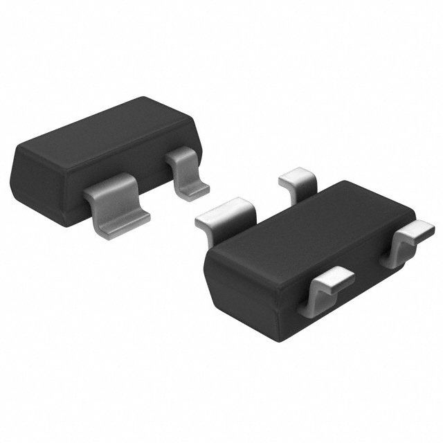
The BFG25A/X is an NPN silicon wideband transistor housed in a four-lead dual emitter SOT143B plastic package. It supports a maximum collector-base voltage of 8 V and a collector-emitter voltage of 5 V, with a DC collector current limit of 6.5 mA. The device features a transition frequency up to 5 GHz and a total power dissipation of 32 mW at a soldering point temperature of 165 °C. Key electrical characteristics include a typical DC current gain of 80 at 0.5 mA and a noise figure as low as 1.8 dB at 1 GHz.
Verify the specific ordering suffix against the manufacturer's latest documentation to confirm availability status and compliance details. Confirm that the SOT143B package dimensions match the design constraints. Ensure the component meets the required environmental standards for the intended deployment environment before finalizing procurement orders.
Select this component for designs requiring wideband operation up to 5 GHz with minimal power draw. Evaluate the thermal resistance of 320 K/W to ensure adequate heat dissipation within the 32 mW limit. Consider the dual emitter configuration for impedance matching requirements in RF amplifier stages operating below 2 GHz.
This part belongs to the BFG series of NPN wideband transistors manufactured by NXP Semiconductors. It utilizes gold metallization technology to enhance long-term reliability compared to standard aluminum metallization alternatives. The SOT143B package provides a compact footprint suitable for space-constrained portable electronic devices.
Consult the official datasheet for cross-reference information regarding compatible substitutes. Verify pinout compatibility and electrical parameter alignment before substituting any alternative components in existing circuit designs.
The maximum unilateral power gain (GUM) is typically 18 dB when the collector current is 0.5 mA, VCE is 1 V, and the ambient temperature is 25 °C.
The feedback capacitance (Cre) decreases as the collector-base voltage increases, dropping from approximately 0.3 pF at low voltages to around 0.21 pF at 1 V under zero bias conditions.
The maximum junction temperature (Tj) is rated at 175 °C.
 BFG25A/X,215
The activity of extra discounts on wholesale prices is in full swing…
Please fill in your contact information and we will send you the latest wholesale price list.