ChipApex | Global Electronic Components Supplier
SEARCH
Search Product
Search Post
— IC芯片 | 连接器 | 传感器 | 被动器件 —
Search productSearch post
— IC芯片 | 连接器 | 传感器 | 被动器件 —
Consult the customer manager about the wholesale price.
consultation hotline:86-132-6715-2157
email:[email protected]
Contact the product manager for consultation. One-stop consultation is available.
Do you want a lower wholesale price? Please send us your inquiry and we will reply immediately.
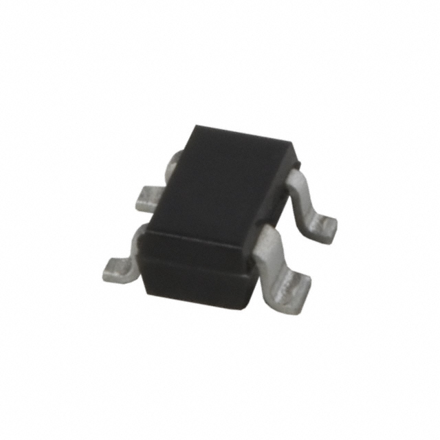
The BFG424F is an NPN double polysilicon wideband transistor featuring a buried layer, designed for low voltage applications. It is housed in a plastic SOT343F package with reverse pinning and four leads. The device supports a collector current of up to 30 mA and a total power dissipation of 135 mW at a solder point temperature of 90 °C. Key electrical characteristics include a transition frequency of 25 GHz, a maximum power gain of 23 dB at 2 GHz, and a noise figure as low as 0.8 dB at 900 MHz. Limiting values specify a collector-base voltage of 10 V and a collector-emitter voltage of 4.5 V.
Verify the component status on the manufacturer's official website before design finalization, as product availability may change. Ensure that handling procedures strictly adhere to ElectroStatic Discharge (ESD) precautions during transport and assembly to prevent device damage. Confirm that the SOT343F package dimensions match the target PCB footprint requirements.
Select this transistor for low voltage RF circuits requiring high gain and low noise performance. Verify that the operating collector current remains within the specified range to maintain optimal transition frequency and power gain characteristics. Ensure the thermal management design keeps the solder point temperature below 90 °C to support the rated total power dissipation limit.
The BFG424F belongs to NXP's portfolio of NPN wideband transistors utilizing double polysilicon technology. This specific model is engineered for cost-effective, high-performance RF solutions in consumer electronics. It complements other discrete RF components by providing reliable amplification in compact surface-mount packages suitable for modern portable devices.
Consult the official NXP datasheet or authorized distributors for verified substitute part numbers. Do not assume functional equivalence with generic NPN transistors without verifying RF parameters such as transition frequency and noise figure against the original specifications.
 BFG424F,115
The activity of extra discounts on wholesale prices is in full swing…
Please fill in your contact information and we will send you the latest wholesale price list.