ChipApex | Global Electronic Components Supplier
SEARCH
Search Product
Search Post
— IC芯片 | 连接器 | 传感器 | 被动器件 —
Search productSearch post
— IC芯片 | 连接器 | 传感器 | 被动器件 —
Consult the customer manager about the wholesale price.
consultation hotline:86-132-6715-2157
email:[email protected]
Contact the product manager for consultation. One-stop consultation is available.
Do you want a lower wholesale price? Please send us your inquiry and we will reply immediately.
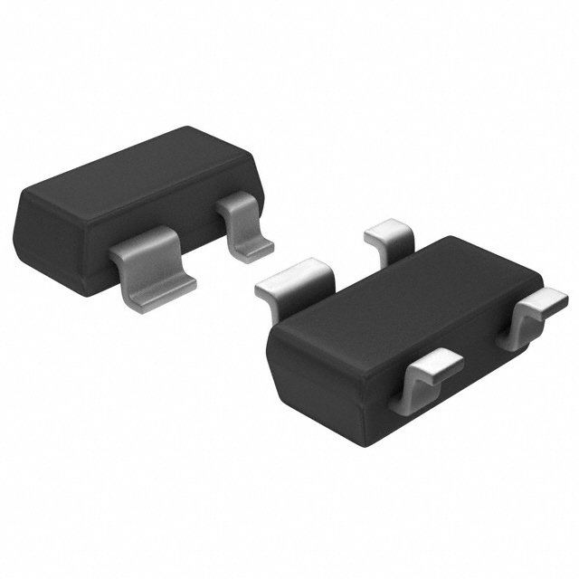
The BFG520/X,215 is an NPN silicon planar epitaxial transistor designed for RF frontend applications in the GHz range. It features a transition frequency of 9 GHz and a maximum unilateral power gain of 19 dB at 900 MHz. The device operates with a collector-emitter voltage of 15 V and a DC collector current limit of 70 mA, dissipating up to 300 mW of total power. Encapsulated in a 4-pin SOT143R surface-mount package, it offers low noise figures starting at 1.1 dB and high reliability through gold metallization.
Verify the specific pin configuration required for the design, as the BFG520/X utilizes reverse pinning compared to the standard BFG520 variant. Confirm that the SOT143R package footprint matches the PCB layout. Ensure the application environment stays within the specified thermal resistance limits to maintain junction temperature below 175 °C during operation.
Select this component when a wideband NPN transistor with high transition frequency is needed for GHz-range signal processing. The BFG520/X is appropriate for designs requiring low noise performance combined with moderate power handling capabilities. Consider the reverse pinout if replacing legacy Philips Semiconductors parts in existing hardware layouts.
This part belongs to the BFG520 family of NPN wideband transistors manufactured by NXP Semiconductors. The 'X' suffix indicates the specific reverse pinning configuration housed in the SOT143R envelope. These devices are successors to earlier Philips Semiconductors products, maintaining identical electrical characteristics while updating branding and documentation standards.
BFG520/XR,215
The primary difference is the pin configuration. The BFG520 uses standard pinning (Collector-Base-Emitter-Emitter), while the BFG520/X uses reverse pinning (Collector-Emitter-Base-Emitter). They share identical electrical specifications.
The maximum junction temperature (Tj) is 175 °C. The total power dissipation is rated at 300 mW up to a soldering point temperature of 88 °C.
At a collector current of 5 mA and VCE of 6 V, the minimum noise figure is typically 1.1 dB at 900 MHz. At 20 mA under the same conditions, it is typically 1.6 dB.
 BFG520/X,215
The activity of extra discounts on wholesale prices is in full swing…
Please fill in your contact information and we will send you the latest wholesale price list.