ChipApex | Global Electronic Components Supplier
SEARCH
Search Product
Search Post
— IC芯片 | 连接器 | 传感器 | 被动器件 —
Search productSearch post
— IC芯片 | 连接器 | 传感器 | 被动器件 —
Consult the customer manager about the wholesale price.
consultation hotline:86-132-6715-2157
email:[email protected]
Contact the product manager for consultation. One-stop consultation is available.
Do you want a lower wholesale price? Please send us your inquiry and we will reply immediately.
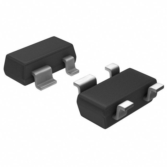
The NXP BFG520/X,235 is an NPN silicon planar epitaxial transistor designed for RF frontend applications in the GHz range. It features a high transition frequency of 9 GHz and excellent power gain characteristics. The device utilizes gold metallization to ensure reliability and is housed in a 4-pin SOT143B plastic surface-mounted package. Key electrical parameters include a collector-base voltage of 20 V, a DC collector current limit of 70 mA, and a total power dissipation of 300 mW at a soldering point temperature up to 88 °C. The typical DC current gain is 120, with a maximum unilateral power gain of 19 dB at 900 MHz.
Verify the specific ordering suffix against the manufacturer's latest documentation to confirm pinning configuration. The BFG520/X variant uses reverse pinning compared to the standard BFG520. Ensure compatibility with the target PCB footprint and thermal management requirements, as the device relies on the collector tab for heat dissipation. Confirm that the application environment remains within the specified junction temperature limits to maintain performance stability.
Select this component when designing RF circuits requiring high transition frequency and low noise figures in the GHz range. The SOT143B package offers a compact solution for space-constrained mobile devices. Consider the thermal resistance from junction to soldering point when calculating power derating curves. Ensure biasing conditions align with the specified DC current and voltage limits to achieve optimal gain and linearity performance without exceeding absolute maximum ratings.
This transistor belongs to the BFG520 family, which includes variants like the BFG520 and BFG520/XR. These devices are engineered for wideband operation in consumer electronics and communication systems. The family shares similar electrical characteristics but differs in pinning arrangements to accommodate various board layout designs. They serve as fundamental building blocks for RF signal processing in portable wireless technologies.
Direct substitutes include the BFG520 and BFG520/XR. Verify pinout compatibility before substitution, as the BFG520/X uses reverse pinning relative to the standard BFG520. Ensure any replacement part meets the same RF performance specifications and package dimensions.
 BFG520/X,235
The activity of extra discounts on wholesale prices is in full swing…
Please fill in your contact information and we will send you the latest wholesale price list.