ChipApex | Global Electronic Components Supplier
SEARCH
Search Product
Search Post
— IC芯片 | 连接器 | 传感器 | 被动器件 —
Search productSearch post
— IC芯片 | 连接器 | 传感器 | 被动器件 —
Consult the customer manager about the wholesale price.
consultation hotline:86-132-6715-2157
email:[email protected]
Contact the product manager for consultation. One-stop consultation is available.
Do you want a lower wholesale price? Please send us your inquiry and we will reply immediately.
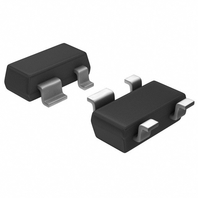
The BFU520VL is an NPN wideband silicon RF transistor from the BFU5 family, designed for high-speed, low-noise applications up to 2 GHz. It utilizes 11 GHz fT technology and features a plastic SOT143B package with dual emitters. Key electrical parameters include a collector-emitter voltage (VCEO) of 12 V, a maximum collector current (IC) of 30 mA, and a total power dissipation (Ptot) of 450 mW at a solder point temperature of 87 °C. The device achieves a minimum noise figure of 0.65 dB at 900 MHz and offers a maximum stable gain of 20 dB at the same frequency.
Verify the specific suffix 'VL' against the official NXP ordering information table to confirm packaging orientation or tape-and-reel specifications. Confirm that the component status remains active or check for obsolescence notices prior to finalizing procurement plans.
Select this component when designing circuits requiring high supply voltages and high breakdown characteristics. Ensure the application board layout supports the thermal resistance requirements specified in the data sheet to maintain junction temperatures within safe operating limits during continuous RF operation.
This part belongs to the BFU5 series of NPN wideband silicon RF transistors manufactured by NXP Semiconductors. The series is engineered for small-signal to medium-power applications, providing a balance of low noise and high gain suitable for various radio frequency circuit designs.
BFU520A
The transition frequency is 10.5 GHz under typical conditions of IC = 10 mA and VCE = 8 V.
The maximum collector-base voltage with the emitter open is 24 V according to the characteristics section.
Yes, the device is AEC-Q101 qualified, indicating it meets automotive electronics council standards for reliability.
 BFU520VL
The activity of extra discounts on wholesale prices is in full swing…
Please fill in your contact information and we will send you the latest wholesale price list.