 ChipApex | Global Electronic Components Supplier
SEARCH
Search Product
Search Post
— IC芯片 | 连接器 | 传感器 | 被动器件 —
Search productSearch post
— IC芯片 | 连接器 | 传感器 | 被动器件 —
Consult the customer manager about the wholesale price.
consultation hotline:86-132-6715-2157
email:[email protected]
Contact the product manager for consultation. One-stop consultation is available.
Do you want a lower wholesale price? Please send us your inquiry and we will reply immediately.
The BG5412KE6327HTSA1 is a dual N-channel MOSFET tetrode designed for the input stages of two-band tuners. It integrates two AGC amplifiers within a single SOT-363 package, featuring an on-chip internal switch controlled by a single line. The device includes integrated gate protection diodes and ESD protection. Key electrical parameters include a drain-source voltage (VDS) of 8 V, continuous drain current (ID) of 25 mA per amplifier, and total power dissipation (Ptot) of 200 mW at case temperatures up to 94 °C. At 800 MHz, it achieves a typical noise figure of 1.1 dB for amplifier A and 1.2 dB for amplifier B.
Verify component authenticity through official Infineon channels or authorized distributors. Confirm that the ordering suffix matches the specific tape-and-reel packaging requirements for automated assembly. Ensure compliance with RoHS directives and AEC-Q101 qualification standards before integration into production designs.
Select this component when designing compact tuner front-ends requiring dual low-noise amplification with gain control. Consider the 8 V maximum drain-source voltage and 25 mA current limits during biasing. Evaluate thermal resistance characteristics if operating near maximum power dissipation limits in high-density PCB layouts.
This part belongs to the BG5412K series of dual MOSFET tetrodes from Infineon Technologies. It is specifically engineered for RF applications where space constraints and signal integrity are critical. The SOT-363 package allows for surface-mount integration in portable electronic devices requiring efficient use of board real estate.
No official substitutes are listed in the datasheet. When evaluating alternatives, verify compatibility regarding pin configuration, maximum voltage ratings, and noise figure specifications. Ensure any replacement maintains the dual-amplifier topology and AGC control interface required by the original circuit design.
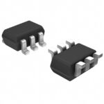 BG5412KE6327HTSA1
The activity of extra discounts on wholesale prices is in full swing…
Please fill in your contact information and we will send you the latest wholesale price list.





