ChipApex | Global Electronic Components Supplier
SEARCH
Search Product
Search Post
— IC芯片 | 连接器 | 传感器 | 被动器件 —
Search productSearch post
— IC芯片 | 连接器 | 传感器 | 被动器件 —
Consult the customer manager about the wholesale price.
consultation hotline:86-132-6715-2157
email:[email protected]
Contact the product manager for consultation. One-stop consultation is available.
Do you want a lower wholesale price? Please send us your inquiry and we will reply immediately.
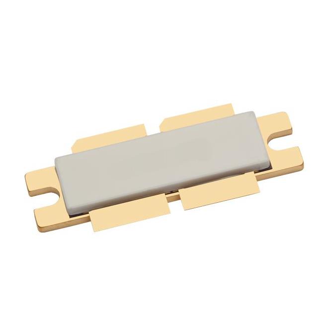
The BLF578,112 is a 1200 W LDMOS power transistor designed for broadcast and industrial applications in the HF to 500 MHz band. It operates with a drain-source voltage of 50 V and features integrated ESD protection. Typical pulsed performance at 225 MHz includes an output power of 1200 W, power gain of 24 dB, and efficiency of 71%. The device exhibits excellent ruggedness, capable of withstanding a VSWR of 13:1 through all phases. It utilizes a flanged balanced ceramic package (SOT539A) with two mounting holes and four leads.
Verify the specific ordering suffix against the manufacturer's current catalog to ensure compatibility with required packaging or testing standards. Confirm that the component meets RoHS Directive 2002/95/EC requirements if hazardous substance restrictions apply to the end product. Always consult the latest product data sheet revision for accurate handling and storage guidelines prior to procurement.
Select this component for high-power RF amplification where broadband coverage from HF to 500 MHz is required. Ensure the design accommodates the 50 V drain supply and manages the thermal resistance of 0.14 K/W junction-to-case. Verify that the application circuit can handle the specified 13:1 VSWR tolerance during class-AB pulsed operation to maintain device integrity.
This part belongs to the Ampleon BLF series of LDMOS power transistors. It is specifically engineered for robust performance in demanding broadcast and industrial environments. The device represents a standard offering for high-power RF generation within its designated frequency band, utilizing established silicon technology for reliable signal amplification.
No direct public substitute part numbers are documented in the provided datasheet. Designers should evaluate other Ampleon BLF series devices with similar power ratings and frequency ranges, ensuring pinout and thermal characteristics match the existing PCB layout.
The device can withstand a load mismatch corresponding to a Voltage Standing-Wave Ratio (VSWR) of 13:1 through all phases under specified pulsed operating conditions.
The gate-source threshold voltage (VGS(th)) is defined with a drain-source voltage of 10 V and a drain current of 500 mA, typically ranging from 1.25 V to 2.25 V.
The typical thermal resistance from junction to case (Rth(j-c)) is 0.14 K/W when measured under RF conditions with a junction temperature of 150 °C.
 BLF578,112
The activity of extra discounts on wholesale prices is in full swing…
Please fill in your contact information and we will send you the latest wholesale price list.