ChipApex | Global Electronic Components Supplier
SEARCH
Search Product
Search Post
— IC芯片 | 连接器 | 传感器 | 被动器件 —
Search productSearch post
— IC芯片 | 连接器 | 传感器 | 被动器件 —
Consult the customer manager about the wholesale price.
consultation hotline:86-132-6715-2157
email:[email protected]
Contact the product manager for consultation. One-stop consultation is available.
Do you want a lower wholesale price? Please send us your inquiry and we will reply immediately.
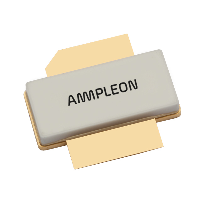
The BLF6G22LS-130 is a 130 W LDMOS power transistor designed for base station applications in the 2000 MHz to 2200 MHz frequency range. It operates at a drain-source voltage of 28 V with a breakdown voltage of 65 V. In a typical 2-carrier W-CDMA test circuit, it delivers an average output power of 30 W with a power gain of 17 dB and a drain efficiency of 28.5%. The device features integrated ESD protection and is internally matched for ease of use. It utilizes an earless flanged SOT502B ceramic package.
Verify the specific ordering suffix against the manufacturer's current product database to confirm availability and exact specifications. Confirm that the component meets all necessary environmental compliance standards required for the intended deployment environment before finalizing procurement orders.
Select this component for designs requiring high ruggedness and thermal stability in cellular infrastructure. Ensure the application circuit can support the specified quiescent current and provides adequate heat sinking to maintain the junction temperature within the recommended operating limits during continuous wave or multi-carrier operations.
This part belongs to the Ampleon BLF series of power LDMOS transistors. It is specifically engineered for wireless communication infrastructure, offering a balance of high power density and linearity suitable for modern wideband modulation schemes used in mobile network base stations.
Consult the official Ampleon replacement guide for verified cross-reference models. Verify pinout compatibility and thermal resistance characteristics when substituting similar devices from other manufacturers to ensure proper integration into existing board layouts.
The absolute maximum drain-source voltage (VDS) rating is 65 V.
Yes, the BLF6G22LS-130 is internally matched to facilitate easier design implementation.
The typical thermal resistance from junction to case (Rth(j-case)) is 0.43 K/W.
 BLF6G22LS-130,118
The activity of extra discounts on wholesale prices is in full swing…
Please fill in your contact information and we will send you the latest wholesale price list.