ChipApex | Global Electronic Components Supplier
SEARCH
Search Product
Search Post
— IC芯片 | 连接器 | 传感器 | 被动器件 —
Search productSearch post
— IC芯片 | 连接器 | 传感器 | 被动器件 —
Consult the customer manager about the wholesale price.
consultation hotline:86-132-6715-2157
email:[email protected]
Contact the product manager for consultation. One-stop consultation is available.
Do you want a lower wholesale price? Please send us your inquiry and we will reply immediately.
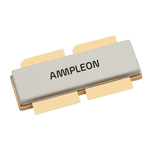
The BLF989SU is a dual N-channel LDMOS RF power transistor designed for broadcast and industrial applications in the 400 MHz to 860 MHz frequency range. It features a drain-source voltage of 50 V, an average output power of 135 W per section (270 W total), and a typical power gain of 22.5 dB at 700 MHz. The device operates with a quiescent current of 650 mA per section and achieves a drain efficiency of up to 35%. It utilizes a SOT539B earless flanged balanced ceramic package.
Verify the specific ordering suffix 'S' corresponds to the SOT539B earless flanged package variant rather than the standard SOT539A version. Confirm RoHS compliance status directly with the manufacturer or authorized distributor as specifications may vary by production batch. Ensure proper handling precautions are observed due to electrostatic sensitivity.
Select this component for high-power UHF applications requiring robust performance in Class-AB broadband or symmetric Doherty configurations. Verify thermal management requirements based on the junction-to-case thermal resistance of 0.13 K/W. Ensure the operating frequency falls within the specified 400 MHz to 860 MHz range for optimal gain and efficiency characteristics.
The BLF989SU belongs to Ampleon's UHF power LDMOS transistor family, specifically engineered for broadcast and industrial sectors. It serves as a high-reliability alternative for digital and analog transmitter designs, offering enhanced stability and power control capabilities compared to previous generation devices.
The BLF989 (SOT539A) is the primary functional equivalent with a different physical package configuration. Direct substitution requires verifying mechanical fit and mounting hole alignment between the flanged SOT539A and earless SOT539B variants.
The device can withstand a load mismatch corresponding to a Voltage Standing Wave Ratio (VSWR) of 40:1 through all phases under specified test conditions.
In a Class-AB broadband application at 700 MHz, the typical drain efficiency is 35%.
The gate-source threshold voltage (VGS(th)) is typically 2.2 V, with a minimum of 1.5 V and a maximum of 2.5 V when measured at VDS = 10 V and ID = 240 mA.
 BLF989SU
The activity of extra discounts on wholesale prices is in full swing…
Please fill in your contact information and we will send you the latest wholesale price list.