 ChipApex | Global Electronic Components Supplier
SEARCH
Search Product
Search Post
— IC芯片 | 连接器 | 传感器 | 被动器件 —
Search productSearch post
— IC芯片 | 连接器 | 传感器 | 被动器件 —
Consult the customer manager about the wholesale price.
consultation hotline:86-132-6715-2157
email:[email protected]
Contact the product manager for consultation. One-stop consultation is available.
Do you want a lower wholesale price? Please send us your inquiry and we will reply immediately.
The BSD235CH6327XTSA1 is a complementary small-signal transistor featuring N-channel and P-channel MOSFETs in an SOT-363-6 package. It operates with a drain-source breakdown voltage of ±20 V. Continuous drain currents are rated at 0.95 A for the N-channel and -0.53 A for the P-channel. The device supports super logic level operation at 2.5 V, has a maximum power dissipation of 500 mW, and functions within a temperature range of -55 °C to +150 °C.
Verify the component against official Infineon documentation to confirm exact specifications and compliance status. Ensure that the ordering suffix matches the required tape and reel packaging format. Cross-reference the specific part number with authorized distribution channels to guarantee authenticity and traceability before finalizing procurement orders.
Select this component when a compact dual-transistor solution is required for low-voltage signal or load switching. The integrated complementary design reduces board space compared to discrete components. Consider the 2.5 V logic level rating for compatibility with standard microcontroller outputs. Evaluate thermal constraints based on the specified power dissipation limits under expected operating conditions.
This component belongs to the BSD235 series from Infineon Technologies. It utilizes OptiMOS™ 2 technology for the N-channel and OptiMOS™-P 2 technology for the P-channel. The series is designed for efficient small-signal switching in automotive and industrial environments requiring high reliability and low profile packaging.
Direct substitutes include BSD235NH6327XTSA1 (N-channel only) and BSD235CH6327XT (same function, different packing). Verify pinout compatibility and electrical ratings before substitution.
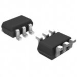 BSD235CH6327XTSA1
The activity of extra discounts on wholesale prices is in full swing…
Please fill in your contact information and we will send you the latest wholesale price list.





