 ChipApex | Global Electronic Components Supplier
SEARCH
Search Product
Search Post
— IC芯片 | 连接器 | 传感器 | 被动器件 —
Search productSearch post
— IC芯片 | 连接器 | 传感器 | 被动器件 —
Consult the customer manager about the wholesale price.
consultation hotline:86-132-6715-2157
email:[email protected]
Contact the product manager for consultation. One-stop consultation is available.
Do you want a lower wholesale price? Please send us your inquiry and we will reply immediately.
The BSD235NH6327XTSA1 is a dual N-channel OptiMOS™2 small-signal transistor in a PG-SOT-363 package. It features a 20 V drain-source breakdown voltage and a continuous drain current of 0.95 A at 25 °C. The device supports super logic level operation with a gate threshold voltage ranging from 0.7 V to 1.2 V, enabling efficient switching at low voltages. It includes avalanche rating capabilities and meets AEC-Q101 automotive qualification standards.
Verify the complete part number including the H6327 suffix to ensure correct packaging specifications. Confirm that the component meets RoHS compliance requirements for your specific manufacturing process. Check the datasheet revision date to ensure alignment with your design documentation. Ensure storage conditions adhere to the specified climatic category limits.
Select this component when a dual N-channel MOSFET with low gate charge and high switching speed is required. The 2.5 V logic level capability makes it suitable for microcontroller-driven applications. Consider the thermal resistance characteristics for PCB layout optimization. Verify that the pulsed drain current ratings align with the expected load transients in the target application.
This component belongs to the BSD235 series of OptiMOS™2 small-signal transistors manufactured by Infineon Technologies. The series is designed for general-purpose switching applications requiring high efficiency and reliability. The PG-SOT-363 package provides a compact footprint suitable for space-constrained designs.
Direct substitutes include BSD235CH6327XTSA1 for mixed polarity configurations. Verify pinout compatibility and electrical parameter overlaps before substitution. Consult official replacement guides for cross-reference information.
The single pulse avalanche energy rating is 1.6 mJ under specified test conditions.
Yes, the component is qualified according to the AEC-Q101 standard for automotive use.
The typical turn-on delay time is 3.8 ns.
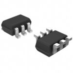 BSD235NH6327XTSA1
The activity of extra discounts on wholesale prices is in full swing…
Please fill in your contact information and we will send you the latest wholesale price list.





