ChipApex | Global Electronic Components Supplier
SEARCH
Search Product
Search Post
— IC芯片 | 连接器 | 传感器 | 被动器件 —
Search productSearch post
— IC芯片 | 连接器 | 传感器 | 被动器件 —
Consult the customer manager about the wholesale price.
consultation hotline:86-132-6715-2157
email:[email protected]
Contact the product manager for consultation. One-stop consultation is available.
Do you want a lower wholesale price? Please send us your inquiry and we will reply immediately.
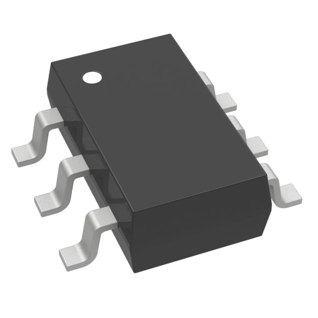
The BSL215PL6327HTSA1 is a dual P-channel OptiMOS™ P2 small-signal transistor in a PG-TSOP6 package. It features Super Logic Level operation rated at 2.5V, with a maximum drain-source voltage of -20V and continuous drain current of -1.5A. The device supports avalanche energy ratings of 11mJ and reverse diode dv/dt of 6kV/µs. Key electrical parameters include an on-state resistance of 150mΩ at VGS=-4.5V and 280mΩ at VGS=-2.5V. Total gate charge is typically 3.55nC.
Verify the specific ordering suffix L6327HTSA1 against official Infineon documentation to confirm tape and reel specifications and marking codes. Ensure compliance with RoHS and halogen-free requirements as stated in the datasheet. Confirm that the PG-TSOP6 package dimensions match your PCB footprint design constraints before finalizing procurement orders.
Select this component when dual P-channel switching is required in a minimal footprint. The 2.5V logic level rating makes it suitable for low-voltage microcontroller interfaces. Consider the thermal resistance of 250K/W and power dissipation limits for ambient temperature conditions. Verify that the -20V breakdown voltage meets the circuit's maximum operating voltage requirements.
This part belongs to Infineon’s OptiMOS™ P2 family of small-signal transistors. These devices are designed for general-purpose switching applications requiring high reliability. The dual configuration allows for efficient space utilization in dense circuit designs. The technology focuses on optimizing on-resistance and switching characteristics for low-power systems.
Check for compatible dual P-channel TSOP6 alternatives from other manufacturers if supply is constrained. Ensure replacement parts meet or exceed the -20V VDS and -1.5A ID ratings. Verify that any substitute also supports Super Logic Level operation at 2.5V if that interface requirement is critical.
The single pulse avalanche energy rating is 11mJ when tested at a drain current of -1.5A and RGS of 25Ω.
Yes, the BSL215P is qualified according to the AEC Q101 standard for automotive applications.
The typical total gate charge (Qg) is 3.55nC under standard test conditions.
 BSL215PL6327HTSA1
The activity of extra discounts on wholesale prices is in full swing…
Please fill in your contact information and we will send you the latest wholesale price list.