ChipApex | Global Electronic Components Supplier
SEARCH
Search Product
Search Post
— IC芯片 | 连接器 | 传感器 | 被动器件 —
Search productSearch post
— IC芯片 | 连接器 | 传感器 | 被动器件 —
Consult the customer manager about the wholesale price.
consultation hotline:86-132-6715-2157
email:[email protected]
Contact the product manager for consultation. One-stop consultation is available.
Do you want a lower wholesale price? Please send us your inquiry and we will reply immediately.
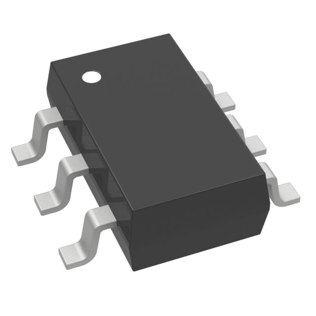
The BSL308CL6327HTSA1 is a dual enhancement-mode MOSFET array from Infineon's OptiMOS series, featuring one P-channel and one N-channel device. It operates with a maximum drain-source voltage of 30 V and supports a continuous drain current of 2.3 A. The component utilizes a TSOP-6 surface-mount package with dimensions of 2.9 mm in length and 1 mm in height. Key electrical parameters include a maximum on-resistance of 57 mΩ, a power dissipation rating of 0.6 W, and a typical gate charge of -5 nC at the specified gate-source voltage. It functions within a temperature range of -55°C to 150°C and complies with AEC-Q101 automotive standards.
Verify the specific suffix against official Infineon documentation to confirm exact binning, tape-and-reel specifications, and RoHS compliance status. Ensure the ordering part number matches the required automotive grade and packaging format before finalizing procurement orders.
Select this component when a matched P-N pair is required for low-voltage, high-efficiency switching applications. The 30 V rating and 2.3 A current capacity suit systems operating within these limits. Verify that the TSOP-6 footprint aligns with the target PCB layout constraints.
This device belongs to the OptiMOS family, designed for optimized power performance in small packages. It serves as a discrete solution for integrating complementary switching elements, reducing board space compared to using separate individual transistors.
The maximum operating junction temperature is 150°C.
Yes, it is qualified according to the AEC-Q101 standard for automotive applications.
 BSL308CL6327HTSA1
The activity of extra discounts on wholesale prices is in full swing…
Please fill in your contact information and we will send you the latest wholesale price list.