ChipApex | Global Electronic Components Supplier
SEARCH
Search Product
Search Post
— IC芯片 | 连接器 | 传感器 | 被动器件 —
Search productSearch post
— IC芯片 | 连接器 | 传感器 | 被动器件 —
Consult the customer manager about the wholesale price.
consultation hotline:86-132-6715-2157
email:[email protected]
Contact the product manager for consultation. One-stop consultation is available.
Do you want a lower wholesale price? Please send us your inquiry and we will reply immediately.
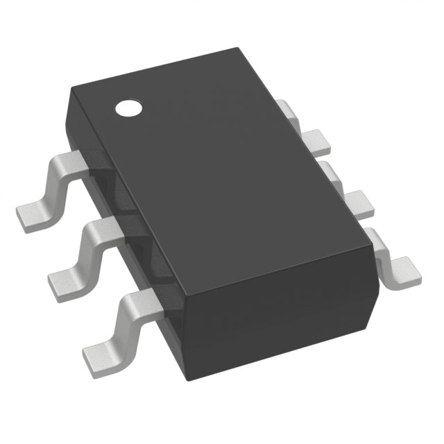
The BSL315PL6327HTSA1 is a dual P-channel OptiMOS-P 2 small-signal transistor in a PG-TSOP-6 package. It features a drain-source breakdown voltage of -30 V and continuous drain current of -1.5 A at 25 °C. The device has a maximum on-state resistance of 150 mΩ at VGS=10 V and 270 mΩ at VGS=4.5 V. It supports pulsed drain currents up to -6 A, operates within a temperature range of -55 °C to +150 °C, and dissipates 0.5 W. The component is avalanche rated with an energy capability of 11 mJ.
Verify the specific ordering suffix H6327 against official Infineon documentation to confirm tape and reel packaging specifications. Ensure the component meets AEC-Q101 qualification requirements if intended for automotive deployment. Cross-reference the full part number with manufacturer databases to validate current production status and availability constraints.
Select this component for designs requiring dual P-channel logic-level switching in a compact surface-mount footprint. Evaluate thermal performance based on the 250 K/W junction-to-ambient resistance under minimal PCB footprint conditions. Confirm that the 150 mΩ on-resistance at 10 V gate drive aligns with system efficiency targets.
This component belongs to the BSL315P series from Infineon Technologies. It utilizes OptiMOS-P 2 technology to provide optimized small-signal performance. The device is designed for general-purpose switching tasks where low on-resistance and high reliability are required in space-constrained environments.
Consult official Infineon cross-reference lists for verified substitutes. Verify pinout compatibility and electrical parameter alignment before substituting.
 BSL315PL6327HTSA1
The activity of extra discounts on wholesale prices is in full swing…
Please fill in your contact information and we will send you the latest wholesale price list.