ChipApex | Global Electronic Components Supplier
SEARCH
Search Product
Search Post
— IC芯片 | 连接器 | 传感器 | 被动器件 —
Search productSearch post
— IC芯片 | 连接器 | 传感器 | 被动器件 —
Consult the customer manager about the wholesale price.
consultation hotline:86-132-6715-2157
email:[email protected]
Contact the product manager for consultation. One-stop consultation is available.
Do you want a lower wholesale price? Please send us your inquiry and we will reply immediately.
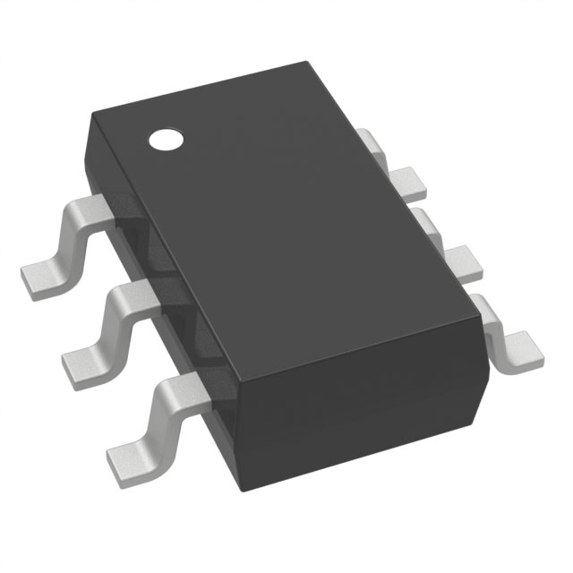
The BSL316CL6327HTSA1 is a dual MOSFET from Infineon Technologies, integrating N-channel and P-channel enhancement mode transistors in a TSOP-6 surface-mount package. It features a drain-source breakdown voltage of 30 V and continuous drain currents of 1.4 A. The device exhibits low on-resistance values of 160 mOhms for the N-channel and 150 mOhms for the P-channel. Gate-source voltage limits are specified at ±20 V, with gate charges of 600 pC and 2.4 nC respectively. Power dissipation is rated at 500 mW, operating within a temperature range of -55 °C to +150 °C.
Verify the exact part number suffix against official Infineon documentation, as availability may vary by region. Confirm RoHS compliance status and automotive qualification requirements before integration. Check for obsolescence notices or lifecycle changes directly from the manufacturer. Ensure supply chain sources provide valid traceability data for quality assurance purposes.
Select this component when space-constrained designs require both N-type and P-type switching capabilities. The TSOP-6 package offers a small footprint suitable for dense PCB layouts. Evaluate thermal performance based on the 500 mW dissipation rating under expected load conditions. Compare on-resistance specifications against system efficiency targets to ensure optimal voltage drop performance.
This device belongs to the BSL316 series of dual MOSFETs designed for general-purpose switching tasks. It utilizes silicon technology to deliver reliable performance in consumer and industrial electronics. The integration of complementary channels simplifies circuit design by reducing component count and board area requirements compared to discrete solutions.
Publicly confirmed substitute part numbers are not available in the provided source material.
 BSL316CL6327HTSA1
The activity of extra discounts on wholesale prices is in full swing…
Please fill in your contact information and we will send you the latest wholesale price list.