 ChipApex | Global Electronic Components Supplier
SEARCH
Search Product
Search Post
— IC芯片 | 连接器 | 传感器 | 被动器件 —
Search productSearch post
— IC芯片 | 连接器 | 传感器 | 被动器件 —
Consult the customer manager about the wholesale price.
consultation hotline:86-132-6715-2157
email:[email protected]
Contact the product manager for consultation. One-stop consultation is available.
Do you want a lower wholesale price? Please send us your inquiry and we will reply immediately.
The BSO4804 is an N-channel enhancement mode power MOSFET from Infineon's OptiMOS/G01 family, housed in a PG-DSO-8-7 package. It features a maximum drain-source voltage of 30 V and a continuous drain current of 8 A at 25°C. The device exhibits a low on-state resistance of 20 mΩ at 10 V gate drive. Key electrical parameters include a total gate charge of 17 nC, input capacitance of 870 pF, and output capacitance of 370 pF. It supports pulsed drain currents up to 32 A and single-pulse avalanche energy of 90 mJ.
Verify the specific ordering code Q67042-S4097 matches the required PG-DSO-8-7 package variant. Confirm RoHS compliance status and Pb-free lead plating specifications align with assembly requirements. Check for any obsolete status or lifecycle notices as the datasheet revision dates back to 2005. Ensure thermal management designs account for the specified junction-to-soldering point thermal resistance values under actual PCB footprint conditions.
Select this component for applications requiring 30 V breakdown with high current handling in a surface-mount format. The logic-level threshold simplifies gate drive design compared to standard threshold devices. Consider the thermal resistance characteristics when designing PCB copper areas for heat dissipation. Evaluate the avalanche energy rating if the application involves significant inductive loads or potential voltage spikes during turn-off.
This part belongs to Infineon's OptiMOS/G01 series, representing early generation optimized power MOSFET technology. The PG-DSO-8-7 package provides a compact solution for moderate power applications. The device integrates monolithic construction for reliability. It serves as a foundational component for low-voltage power switching architectures where efficiency and switching speed are prioritized alongside cost-effectiveness.
No public confirmed substitute part numbers are available in the provided documentation.
The device is rated for 90 mJ of single-pulse avalanche energy under conditions of ID=8 A, VDD=25 V, and RGS=25 Ω.
The gate threshold voltage decreases as junction temperature increases, ranging from a minimum of 1.2 V to a maximum of 2 V at 25°C, with typical behavior showing negative temperature coefficient.
The reverse recovery time (trr) is typically 24 ns and maximally 30 ns when measured at VR=15 V, IF=IS, and diF/dt=100 A/µs.
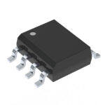 BSO4804T
The activity of extra discounts on wholesale prices is in full swing…
Please fill in your contact information and we will send you the latest wholesale price list.





